
5SGXEA5N2F40C1G
| Part Description |
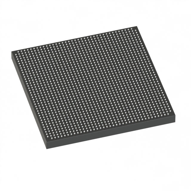
Stratix® V GX Field Programmable Gate Array (FPGA) IC 600 46080000 490000 1517-BBGA, FCBGA |
|---|---|
| Quantity | 514 Available (as of June 10, 2026) |

| Product Category | Field Programmable Gate Array (FPGA) |
|---|---|
| Manufacturer | Intel |
| Manufacturing Status | Active |
| Manufacturer Standard Lead Time | 26 Weeks |
| Datasheet |
Specifications & Environmental
| Device Package | 1517-FBGA (40x40) | Grade | Commercial | Operating Temperature | 0°C – 85°C | ||
|---|---|---|---|---|---|---|---|
| Package / Case | 1517-BBGA, FCBGA | Number of I/O | 600 | Voltage | 870 mV - 930 mV | ||
| Mounting Method | Surface Mount | RoHS Compliance | RoHS Compliant | REACH Compliance | REACH Unaffected | ||
| Moisture Sensitivity Level | 3 (168 Hours) | Number of LABs/CLBs | 185000 | Number of Logic Elements/Cells | 490000 | ||
| Number of Gates | N/A | ECCN | N/A | HTS Code | N/A | ||
| Qualification | N/A | Total RAM Bits | 46080000 |
Overview of 5SGXEA5N2F40C1G – Stratix® V GX Field Programmable Gate Array (FPGA) IC 600 46080000 490000 1517-BBGA, FCBGA
The 5SGXEA5N2F40C1G is a Stratix V GX family FPGA offered in a 1517-BBGA FCBGA surface-mount package. It delivers a high-density programmable fabric with large embedded memory and extensive I/O capacity for demanding digital designs.
Designed for commercial-grade applications, this device targets systems that require broad logic resources, significant on-chip RAM, and high pin-count connectivity—suitable for communications, compute acceleration, and complex system integration.
Key Features
- High logic capacity — Approximately 490,000 logic elements to implement large state machines, datapaths, and custom processing pipelines.
- Significant embedded memory — Approximately 46 Mbits of on-chip RAM for buffering, FIFO, and LUT-based storage needs.
- Extensive I/O — 600 I/O pins to support wide external interfacing and multi-channel connectivity.
- High-speed transceiver family capability — As a Stratix V GX device, the family supports transceiver channel rates up to 14.1 Gbps; consult the device datasheet for available transceiver speed-grade options.
- Low-voltage core — Core supply range 0.87 V to 0.93 V to match modern low-voltage system domains.
- Commercial temperature grade — Rated for operation from 0°C to 85°C for standard commercial deployments.
- Compact FCBGA package — 1517-ball BBGA (supplier package: 1517-FBGA, 40×40) in a surface-mount format for high pin count and dense PCB layouts.
- RoHS compliant — Conforms to RoHS requirements for lead-free assembly processing.
Typical Applications
- High-speed communications — Implement multi-channel transceiver interfaces and protocol processing leveraging the Stratix V GX transceiver capabilities and high I/O count.
- Network and data-plane acceleration — Use the large logic element count and embedded memory for packet processing, classification, and custom accelerator functions.
- Compute and signal processing — Deploy wide datapaths and parallel processing pipelines that take advantage of the device’s logic density and on-chip RAM.
- System integration and prototyping — Integrate complex glue logic, high-pin-count peripherals, and memory interfaces in a single FPGA package for rapid system development.
Unique Advantages
- High-density programmable fabric: Approximately 490,000 logic elements enable implementation of large, complex designs without partitioning across multiple devices.
- Large embedded memory: Approximately 46 Mbits of on-chip RAM reduces external memory dependence and simplifies timing-critical buffering.
- Broad external connectivity: 600 I/Os provide flexibility for multi-channel interfaces, wide buses, and mixed-signal front-ends.
- Family-level transceiver support: Stratix V GX family transceivers support multi-gigabit channel rates (up to 14.1 Gbps), enabling high-bandwidth serial links when matched to the required speed grade.
- Compact, manufacturable package: 1517-ball FCBGA surface-mount package delivers high pin count in a PCB-friendly footprint for production assemblies.
- Commercial-grade operating range: 0°C to 85°C supports standard commercial deployments and system environments.
Why Choose 5SGXEA5N2F40C1G?
The 5SGXEA5N2F40C1G positions itself as a high-capacity, commercially rated Stratix V GX FPGA that balances large programmable logic, substantial on-chip memory, and extensive I/O in a compact FCBGA package. It is suited to designers building high-throughput communications, compute acceleration, and complex integration tasks that require dense logic and memory resources.
Choosing this device provides a scalable platform within the Stratix V GX family—offering the logic and memory resources necessary for advanced designs while aligning with standard commercial temperature and low-voltage core domains.
Request a quote or submit an inquiry to check pricing and availability for the 5SGXEA5N2F40C1G and to discuss how this Stratix V GX device can meet your project requirements.


Date Founded: 1968
Headquarters: Santa Clara, California, USA
Employees: 130,000+
Revenue: $54.23 Billion
Certifications and Memberships: ISO9001:2015, ISO14001:2015, ISO17025:2017, ISO27001:2022, ISO45001:2018, ISO50001:2018


