
5SGXEA5N1F45C2LN
| Part Description |
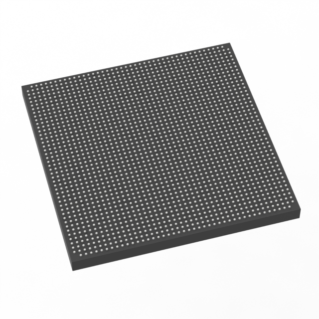
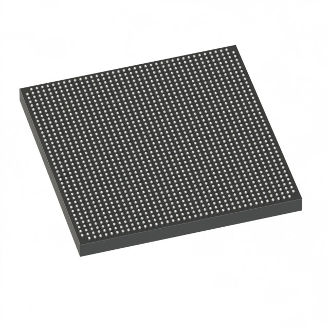
Stratix® V GX Field Programmable Gate Array (FPGA) IC 840 46080000 490000 1932-BBGA, FCBGA |
|---|---|
| Quantity | 597 Available (as of June 15, 2026) |

| Product Category | Field Programmable Gate Array (FPGA) |
|---|---|
| Manufacturer | Intel |
| Manufacturing Status | Obsolete |
| Manufacturer Standard Lead Time | Contact Us |
| Datasheet |
Specifications & Environmental
| Device Package | 1932-FBGA, FC (45x45) | Grade | Commercial | Operating Temperature | 0°C – 85°C | ||
|---|---|---|---|---|---|---|---|
| Package / Case | 1932-BBGA, FCBGA | Number of I/O | 840 | Voltage | 820 mV - 880 mV | ||
| Mounting Method | Surface Mount | RoHS Compliance | RoHS Compliant | REACH Compliance | REACH Unknown | ||
| Moisture Sensitivity Level | 3 (168 Hours) | Number of LABs/CLBs | 185000 | Number of Logic Elements/Cells | 490000 | ||
| Number of Gates | N/A | ECCN | 3A001A2C | HTS Code | 8542.39.0001 | ||
| Qualification | N/A | Total RAM Bits | 46080000 |
Overview of 5SGXEA5N1F45C2LN – Stratix® V GX FPGA, 490,000 Logic Elements, 840 I/Os
The 5SGXEA5N1F45C2LN is a Stratix V GX fieldprogrammable gate array (FPGA) IC from Intel, offered in a 1932-ball FCBGA package. It provides a high-density programmable fabric and on-chip memory for complex digital designs that require large logic capacity and extensive I/O.
Designed for commercial-temperature applications, this device targets designs that demand a combination of high logic element count, substantial embedded RAM, and broad I/O connectivity while operating from a low-voltage core supply.
Key Features
- Logic Capacity Approximately 490,000 logic elements, enabling large-scale integration of custom digital functions on a single device.
- Embedded Memory Approximately 46 Mbits of on-chip RAM to support buffering, packet processing, and data-heavy algorithms without immediate dependence on external memory.
- I/O Density 840 user I/Os to accommodate complex board-level interfacing and multi-channel connectivity.
- Transceiver and Timing (Device Family) Stratix V GX family documentation includes transceiver speed grade options (family-level information includes GX channel speeds reported in device documentation), supporting high-speed serial connectivity as specified in the Stratix V device datasheet.
- Power Core voltage supply range: 820 mV to 880 mV, allowing low-voltage core operation consistent with the Stratix V device requirements.
- Package and Mounting 1932-ball BGA (1932-BBGA, FCBGA); supplier device package listed as 1932-FBGA, FC (45×45). Surface-mount mounting type for standard PCB assembly.
- Operating Range Commercial grade operation rated from 0 °C to 85 °C for typical commercial-environment deployments.
- RoHS Compliance Device is RoHS compliant, meeting common lead-free environmental requirements.
Typical Applications
- High-density custom digital processing Complex algorithms and state machines that require up to 490,000 logic elements and substantial embedded RAM.
- High-throughput communications Designs leveraging Stratix V GX transceiver options documented for high-speed serial channels as part of the device family.
- Large I/O systems Multi-channel data acquisition, control systems, or board-level subsystems that need up to 840 I/Os for sensors, peripherals, and external interfaces.
Unique Advantages
- High logic density: Combines approximately 490,000 logic elements to consolidate complex digital functions onto a single FPGA.
- Significant on-chip memory: Approximately 46 Mbits of embedded RAM reduces dependency on external memory for many buffering and data-processing tasks.
- Extensive I/O count: 840 I/Os support rich connectivity options for multi-channel and multi-peripheral designs.
- Compact FCBGA package: 1932-ball FCBGA footprint delivers the device density required for space-constrained, high-performance PCBs.
- Low-voltage core operation: 820 mV–880 mV core supply range aligns with the Stratix V device family’s power architecture.
- Commercial temperature rating: Rated 0 °C to 85 °C for designs targeting commercial environments.
Why Choose 5SGXEA5N1F45C2LN?
The 5SGXEA5N1F45C2LN positions itself as a high-density Stratix V GX FPGA option for commercial applications that require a large number of logic elements, substantial on-chip memory, and a high I/O count in a single surface-mount FCBGA package. Its specification set—490,000 logic elements, approximately 46 Mbits of embedded RAM, 840 I/Os, and a low-voltage core supply—makes it suitable for complex digital designs and high-throughput systems.
Backed by Intel’s Stratix V device documentation, this FPGA is appropriate for engineers and teams looking to scale logic and memory resources in commercial-temperature designs while leveraging a documented family of transceiver and timing options.
If you need pricing, availability, or a custom quote for 5SGXEA5N1F45C2LN, request a quote or submit an inquiry to receive detailed ordering and lead-time information.


Date Founded: 1968
Headquarters: Santa Clara, California, USA
Employees: 130,000+
Revenue: $54.23 Billion
Certifications and Memberships: ISO9001:2015, ISO14001:2015, ISO17025:2017, ISO27001:2022, ISO45001:2018, ISO50001:2018


