
5SGXEA5N1F45I2G
| Part Description |
Stratix® V GX Field Programmable Gate Array (FPGA) IC 840 46080000 490000 1932-BBGA, FCBGA |
|---|---|
| Quantity | 1,036 Available (as of June 15, 2026) |

| Product Category | Field Programmable Gate Array (FPGA) |
|---|---|
| Manufacturer | Intel |
| Manufacturing Status | Active |
| Manufacturer Standard Lead Time | 26 Weeks |
| Datasheet |
Specifications & Environmental
| Device Package | 1932-FBGA, FC (45x45) | Grade | Industrial | Operating Temperature | -40°C – 100°C | ||
|---|---|---|---|---|---|---|---|
| Package / Case | 1932-BBGA, FCBGA | Number of I/O | 840 | Voltage | 870 mV - 930 mV | ||
| Mounting Method | Surface Mount | RoHS Compliance | RoHS Compliant | REACH Compliance | REACH Unaffected | ||
| Moisture Sensitivity Level | 3 (168 Hours) | Number of LABs/CLBs | 185000 | Number of Logic Elements/Cells | 490000 | ||
| Number of Gates | N/A | ECCN | N/A | HTS Code | N/A | ||
| Qualification | N/A | Total RAM Bits | 46080000 |
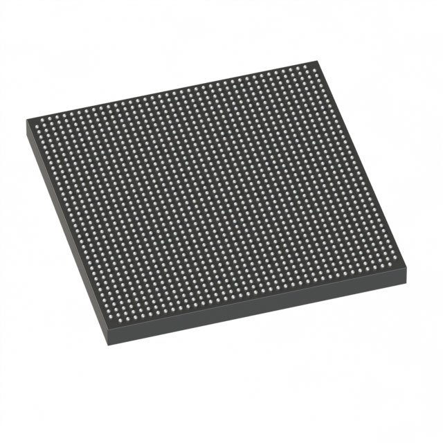
Overview of 5SGXEA5N1F45I2G – Stratix® V GX FPGA — 490,000 logic elements, 840 I/Os
The 5SGXEA5N1F45I2G is an Intel Stratix V GX field programmable gate array (FPGA) offered in an industrial-grade package. It delivers a high logic capacity and dense I/O for demanding designs that require substantial on-chip memory and connectivity.
As part of the Stratix V GX family, this device is suited to applications that benefit from large embedded memory, high I/O counts, and industrial temperature operation while providing the supply and packaging options required for board-level integration.
Key Features
- Core Logic — 490,000 logic elements for complex logic integration and large-scale FPGA designs.
- Embedded Memory — approximately 46 Mbits of embedded memory (46,080,000 total RAM bits) to support buffers, FIFOs, and on-chip data storage.
- I/O Density — 840 I/Os to accommodate dense interfacing and multi-channel connectivity.
- Package & Mounting — 1932-BBGA (FCBGA) package; supplier device package listed as 1932-FBGA, FC (45×45); surface-mount mounting for compact board integration.
- Power Supply — Core voltage supply range 870 mV to 930 mV for defined power sequencing and design planning.
- Temperature & Grade — Industrial grade with an operating temperature range of −40°C to 100°C for deployment in industrial environments.
- Standards Compliance — RoHS compliant.
- Family Transceiver Options (datasheet) — The Stratix V GX family datasheet lists GX transceiver speed grades up to 14.1 Gbps, reflecting available high-speed transceiver capability across the family.
Typical Applications
- High-density signal processing — Large logic capacity and substantial on-chip RAM make this FPGA suitable for complex DSP, filtering, and real-time processing pipelines.
- Telecommunications and networking — High I/O count and family transceiver options noted in the datasheet support multi-channel interfacing and high-bandwidth links in infrastructure equipment.
- Data center acceleration — Dense logic and memory resources enable offload and acceleration functions in compute or storage systems.
- Industrial control and automation — Industrial temperature rating and robust packaging support deployment in factory automation and control systems.
Unique Advantages
- Large programmable fabric — 490,000 logic elements reduce the need for multiple devices, simplifying board-level design and lowering BOM complexity.
- Significant on-chip memory — Approximately 46 Mbits of embedded RAM supports deep buffering and high-throughput data paths without relying on external memory.
- High I/O capacity — 840 I/Os enable broad peripheral and multi-channel connectivity directly to the FPGA.
- Industrial-grade operation — Specified −40°C to 100°C operating range and industrial grade classification allow reliable operation in harsh environments.
- Packaged for dense designs — 1932-ball FCBGA footprint provides a high pin-count solution in a compact package suitable for surface-mount assembly.
Why Choose 5SGXEA5N1F45I2G?
The 5SGXEA5N1F45I2G balances large-scale programmable logic, substantial embedded memory, and high I/O density in an industrial-grade Stratix V GX device. Its defined core supply range and FCBGA packaging support integration into complex, high-performance systems where on-chip resources and robust operation are required.
This device is well suited to engineers designing signal processing, networking, data-acceleration, or industrial control systems who need a scalable FPGA platform with clear electrical and thermal operating parameters and family-level transceiver options documented in the datasheet.
Request a quote or submit an inquiry to receive pricing and availability for 5SGXEA5N1F45I2G.


Date Founded: 1968
Headquarters: Santa Clara, California, USA
Employees: 130,000+
Revenue: $54.23 Billion
Certifications and Memberships: ISO9001:2015, ISO14001:2015, ISO17025:2017, ISO27001:2022, ISO45001:2018, ISO50001:2018


