
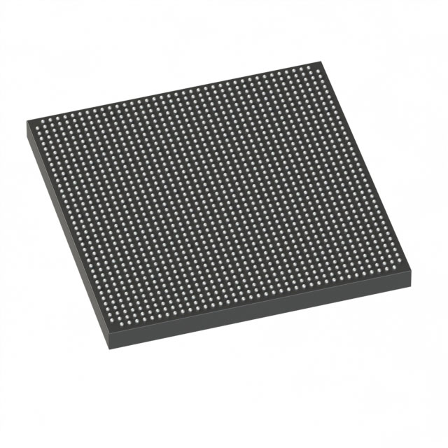
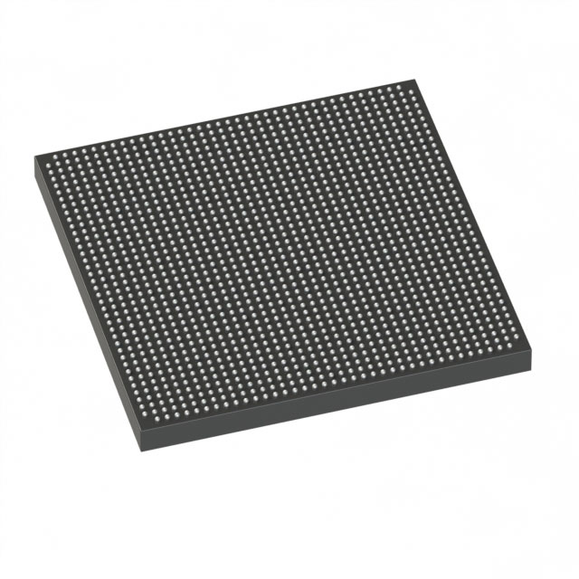
5SGXEA5N3F40C2N
| Part Description |
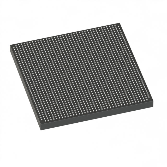
Stratix® V GX Field Programmable Gate Array (FPGA) IC 600 46080000 490000 1517-BBGA, FCBGA |
|---|---|
| Quantity | 250 Available (as of October 7, 2026) |
| Product Category | Field Programmable Gate Array (FPGA) |
|---|---|
| Manufacturer | Intel |
| Manufacturing Status | Obsolete |
| Manufacturer Standard Lead Time | Contact Us |
| Datasheet |
Specifications & Environmental
| Device Package | 1517-FBGA (40x40) | Grade | Commercial | Operating Temperature | 0°C – 85°C | ||
|---|---|---|---|---|---|---|---|
| Package / Case | 1517-BBGA, FCBGA | Number of I/O | 600 | Voltage | 870 mV - 930 mV | ||
| Mounting Method | Surface Mount | RoHS Compliance | RoHS Compliant | REACH Compliance | REACH Unknown | ||
| Moisture Sensitivity Level | 3 (168 Hours) | Number of LABs/CLBs | 185000 | Number of Logic Elements/Cells | 490000 | ||
| Number of Gates | N/A | ECCN | 3A001A2C | HTS Code | 8542.39.0001 | ||
| Qualification | N/A | Total RAM Bits | 46080000 |
Overview of 5SGXEA5N3F40C2N – Stratix® V GX Field Programmable Gate Array (FPGA) IC 600 46080000 490000 1517-BBGA, FCBGA
The 5SGXEA5N3F40C2N is a Stratix® V GX field programmable gate array (FPGA) from Intel designed for applications that require large FPGA capacity and extensive I/O. This commercial‑grade device integrates a high logic element count, substantial on‑chip RAM, and a high I/O count in a 1517‑ball FCBGA package for surface‑mount assembly.
Key attributes include approximately 490,000 logic elements, roughly 46.08 Mbits of embedded memory, and 600 I/Os, enabling complex logic, memory buffering, and broad external interfacing while operating within a core supply range of 870 mV to 930 mV and a commercial temperature range of 0 °C to 85 °C.
Key Features
- Core & Logic Approximately 490,000 logic elements providing substantial programmable logic capacity for large designs and complex algorithms.
- Logic Array Capacity Organized across about 185,000 logic array blocks to structure logic resources for scalable design partitioning.
- Embedded Memory Approximately 46.08 Mbits of on‑chip RAM for data buffering, FIFOs, and state storage without external memory dependence.
- I/O Density 600 user I/Os to support wide parallel interfaces, high‑pin‑count connectors, and multi‑channel systems integration.
- Package & Mounting 1517‑BBGA (FCBGA) 40×40 supplier package in a surface‑mount form factor for high‑density board designs.
- Power Core supply operating range from 870 mV to 930 mV to match regulated FPGA core rails and power‑delivery designs.
- Temperature & Grade Commercial temperature grade rated from 0 °C to 85 °C for use in standard commercial equipment and environments.
- Environmental Compliance RoHS compliant, suitable for designs requiring restricted‑substance adherence.
Typical Applications
- High‑density logic systems Large logic capacity supports complex control, signal processing, and custom accelerators that need extensive programmable resources.
- Memory‑intensive designs Approximately 46.08 Mbits of embedded RAM enables local buffering and data staging for streaming or packetized workloads.
- Multi‑interface platforms 600 I/Os provide the channel and bus density required for systems with numerous parallel peripherals or high connector counts.
- Prototyping and development Commercial‑grade temperature range and a standard FCBGA package make the device suitable for lab and production prototypes targeting commercial products.
Unique Advantages
- Large programmable fabric: High logic element count enables consolidation of multi‑function designs onto a single FPGA, reducing system complexity.
- Significant on‑chip memory: Nearly 46.08 Mbits of embedded RAM reduces dependence on external memory, improving throughput and latency for data‑heavy tasks.
- Extensive I/O capacity: 600 I/Os simplify board routing and support connectivity to many peripherals or parallel interfaces without external multiplexing.
- Compact board footprint: 1517‑ball FCBGA 40×40 package offers high integration in a surface‑mount package suitable for dense PCBs.
- Commercial readiness: Rated for 0 °C to 85 °C and RoHS compliant for standard commercial product deployments.
- Tight core supply window: Defined 870 mV–930 mV core supply supports predictable power‑delivery design and regulator selection.
Why Choose 5SGXEA5N3F40C2N?
The 5SGXEA5N3F40C2N positions itself as a high‑capacity Stratix V GX FPGA option for designers who need a combination of extensive logic resources, sizable embedded memory, and a large number of I/Os in a production‑grade commercial package. Its specifications support consolidation of complex functions and high‑bandwidth board interfacing while maintaining predictable power and thermal parameters.
This device is well suited to design teams building commercial equipment that require scalability, substantial on‑chip resources, and compliance with RoHS requirements, backed by Intel’s Stratix V family documentation and device engineering data.
Request a quote or submit your RFQ today to begin specifying the 5SGXEA5N3F40C2N for your next design.





















Date Founded: 1968
Headquarters: Santa Clara, California, USA
Employees: 130,000+
Revenue: $54.23 Billion
Certifications and Memberships: ISO9001:2015, ISO14001:2015, ISO17025:2017, ISO27001:2022, ISO45001:2018, ISO50001:2018


