
5SGXEA5N3F40C4N
| Part Description |
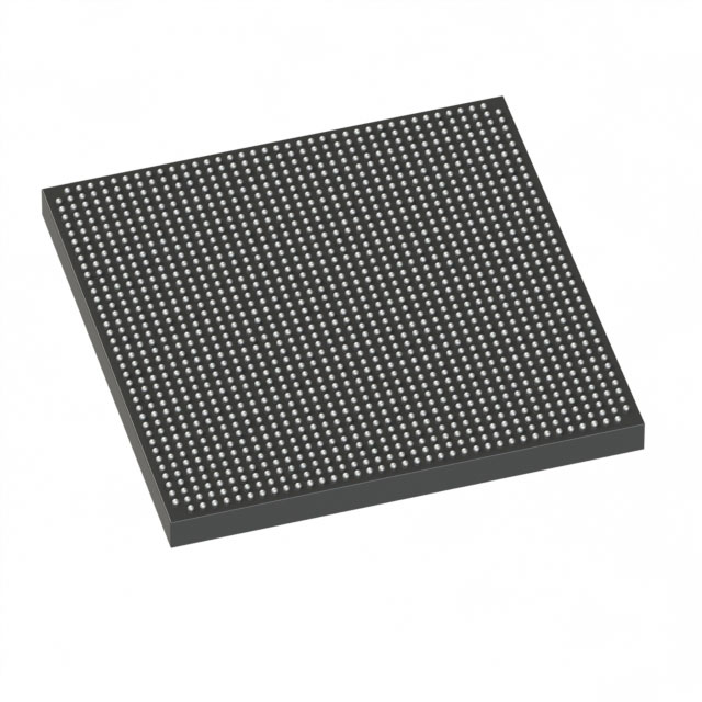
Stratix® V GX Field Programmable Gate Array (FPGA) IC 600 46080000 490000 1517-BBGA, FCBGA |
|---|---|
| Quantity | 22 Available (as of June 16, 2026) |

| Product Category | Field Programmable Gate Array (FPGA) |
|---|---|
| Manufacturer | Intel |
| Manufacturing Status | Obsolete |
| Manufacturer Standard Lead Time | Contact Us |
| Datasheet |
Specifications & Environmental
| Device Package | 1517-FBGA (40x40) | Grade | Commercial | Operating Temperature | 0°C – 85°C | ||
|---|---|---|---|---|---|---|---|
| Package / Case | 1517-BBGA, FCBGA | Number of I/O | 600 | Voltage | 820 mV - 880 mV | ||
| Mounting Method | Surface Mount | RoHS Compliance | RoHS Compliant | REACH Compliance | REACH Unknown | ||
| Moisture Sensitivity Level | 3 (168 Hours) | Number of LABs/CLBs | 185000 | Number of Logic Elements/Cells | 490000 | ||
| Number of Gates | N/A | ECCN | 3A001A2C | HTS Code | 8542.39.0001 | ||
| Qualification | N/A | Total RAM Bits | 46080000 |
Overview of 5SGXEA5N3F40C4N – Stratix® V GX Field Programmable Gate Array (FPGA) IC
The 5SGXEA5N3F40C4N is a Stratix V GX family FPGA delivering high-density programmable logic with extensive I/O and on-chip memory for complex digital systems. This commercial-grade device integrates a large logic fabric, substantial embedded RAM, and support for Stratix V GX transceiver speed grades as documented in the device datasheet.
Designed for surface-mount deployment in a 1517-BBGA (1517-FBGA, 40×40) package, the device offers 600 I/Os and operates across a commercial temperature range with a low-voltage core supply.
Key Features
- Core Logic Approximately 490,000 logic elements for implementating large-scale, complex logic and control functions.
- Embedded Memory Approximately 46 Mbits of on-chip RAM (46,080,000 total RAM bits) to support data buffering, FIFOs, and memory-intensive designs.
- I/O Density Up to 600 general-purpose I/Os to accommodate wide parallel buses, external interfaces, and dense board-level connectivity.
- Transceiver Options Stratix V GX devices are offered with transceiver speed grades documented in the device datasheet (examples include GX channel options up to 14.1 Gbps), enabling high-speed serial links where required.
- Power Domain Core supply voltage range: 820 mV to 880 mV, aligning with modern low-voltage FPGA core domains.
- Package & Mounting 1517-BBGA / FCBGA package (supplier device package: 1517-FBGA, 40×40) with surface-mount mounting suitable for compact board designs.
- Commercial Grade & Temperature Commercial temperature grade with an operating ambient range of 0 °C to 85 °C.
- Environmental Compliance RoHS compliant.
Typical Applications
- High-speed Serial Communications Implement multi-gigabit links using the Stratix V GX transceiver speed grades documented for the family.
- High-density Digital Systems Deploy complex control, DSP, and custom logic functions that require approximately 490k logic elements.
- I/O-Intensive Controllers Systems needing broad external connectivity can leverage up to 600 I/Os for parallel interfaces, sensors, and peripherals.
- Memory-dependent Designs Use the device’s approximately 46 Mbits of embedded memory for buffering, packet queues, and on-chip data structures.
Unique Advantages
- High logic capacity: Approximately 490,000 logic elements enable large, integrated designs and reduce partitioning across multiple devices.
- Significant embedded RAM: Approximately 46 Mbits of on-chip memory reduces reliance on external memory for many buffering and data-path needs.
- Generous I/O count: 600 I/Os support complex board-level connectivity and multiple parallel interfaces without additional I/O expanders.
- Configurable high-speed transceivers: Family transceiver speed grades documented in the Stratix V datasheet support demanding serial communication rates.
- Compact FCBGA package: 1517-BBGA (1517-FBGA, 40×40) surface-mount package enables high-density PCB layouts.
- Commercial temperature and RoHS compliance: 0 °C to 85 °C operating range and RoHS compliance for mainstream commercial applications.
Why Choose 5SGXEA5N3F40C4N?
The 5SGXEA5N3F40C4N brings together a high count of logic elements, substantial embedded memory, and extensive I/O in a compact FCBGA package, making it well suited for complex commercial designs that require significant on-chip resources. Its inclusion in the Stratix V GX family provides access to documented transceiver speed grades for systems requiring high-speed serial connectivity.
For design teams focused on integration density, on-chip memory capacity, and a broad I/O footprint within a commercial-temperature product, this Stratix V GX device delivers a balanced combination of programmable logic resources and package-level integration backed by the Stratix V device documentation.
Request a quote or submit a pricing and availability inquiry for part number 5SGXEA5N3F40C4N to begin specifying this device into your next design.


Date Founded: 1968
Headquarters: Santa Clara, California, USA
Employees: 130,000+
Revenue: $54.23 Billion
Certifications and Memberships: ISO9001:2015, ISO14001:2015, ISO17025:2017, ISO27001:2022, ISO45001:2018, ISO50001:2018


