
5SGXEA5N3F40C4G
| Part Description |
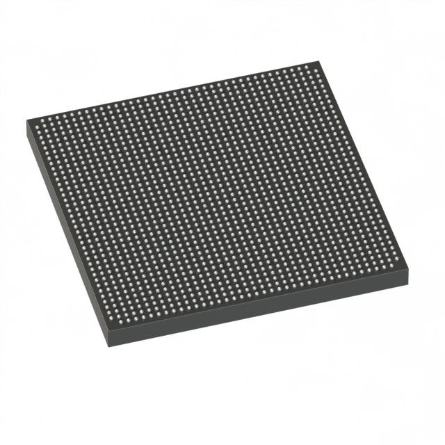
Stratix® V GX Field Programmable Gate Array (FPGA) IC 600 46080000 490000 1517-BBGA, FCBGA |
|---|---|
| Quantity | 1,347 Available (as of June 16, 2026) |

| Product Category | Field Programmable Gate Array (FPGA) |
|---|---|
| Manufacturer | Intel |
| Manufacturing Status | Active |
| Manufacturer Standard Lead Time | 26 Weeks |
| Datasheet |
Specifications & Environmental
| Device Package | 1517-FBGA (40x40) | Grade | Commercial | Operating Temperature | 0°C – 85°C | ||
|---|---|---|---|---|---|---|---|
| Package / Case | 1517-BBGA, FCBGA | Number of I/O | 600 | Voltage | 820 mV - 880 mV | ||
| Mounting Method | Surface Mount | RoHS Compliance | RoHS Compliant | REACH Compliance | REACH Unaffected | ||
| Moisture Sensitivity Level | 3 (168 Hours) | Number of LABs/CLBs | 185000 | Number of Logic Elements/Cells | 490000 | ||
| Number of Gates | N/A | ECCN | N/A | HTS Code | N/A | ||
| Qualification | N/A | Total RAM Bits | 46080000 |
Overview of 5SGXEA5N3F40C4G – Stratix® V GX Field Programmable Gate Array (FPGA) IC
The 5SGXEA5N3F40C4G is an Intel Stratix V GX family Field Programmable Gate Array (FPGA) offered in a 1517-BBGA (40×40 FCBGA) package for surface mount applications. It combines very large logic capacity, substantial on-chip embedded memory, and extensive I/O to support dense, I/O‑rich designs in commercial temperature environments.
This device targets designs that require high logic density and flexible I/O: the device provides 490,000 logic elements, approximately 46.08 Mbits of embedded RAM, and up to 600 I/O pins, while operating from an 820 mV to 880 mV core supply and within a commercial temperature range of 0 °C to 85 °C.
Key Features
- Core Logic — 490,000 logic elements to implement large-scale digital designs and complex custom logic functions.
- Logic Blocks — 185,000 logic block units (as listed) to structure and partition designs for performance and routing efficiency.
- Embedded Memory — Approximately 46.08 Mbits of on-chip RAM for buffering, FIFOs, and memory-intensive functions.
- I/O Density — Up to 600 user I/O pins to support broad external connectivity and parallel interfaces.
- Power — Core supply range of 820 mV to 880 mV; designed for surface-mount implementation.
- Package — 1517-BBGA, FCBGA (listed supplier package: 1517-FBGA, 40×40) delivering a compact, high‑pin‑count footprint.
- Temperature Grade — Commercial grade with an operating temperature range of 0 °C to 85 °C.
- Compliance — RoHS compliant.
Typical Applications
- High-speed serial communication: Stratix V GX series devices include transceiver capabilities suitable for multi‑gigabit serial links (series-level transceiver specifications are provided in the device datasheet).
- Custom accelerators and compute offload: Large logic capacity and substantial on-chip RAM enable hardware acceleration, DSP blocks, and specialized compute engines.
- I/O‑intensive systems: Up to 600 I/O pins support wide parallel buses, extensive peripheral interfacing, and multi-channel I/O aggregation.
- Commercial embedded systems: The commercial temperature grade and surface-mount 1517-BBGA package suit compact, board‑level deployments in commercial products.
Unique Advantages
- High logic density: 490,000 logic elements provide room for complex, large-scale designs without immediate migration to higher-tier devices.
- Significant on‑chip memory: Approximately 46.08 Mbits of embedded RAM reduces the need for external memory in many buffering and storage use cases.
- Extensive I/O capability: 600 I/O pins simplify system integration where multiple peripherals, buses, or channels are required.
- Compact, high‑pin package: The 1517-BBGA FCBGA package offers a dense footprint for high-pin-count implementations in board-constrained designs.
- Commercial temperature operation: Rated for 0 °C to 85 °C to match typical commercial product environments and deployments.
- RoHS compliant: Meets RoHS requirements for broad market acceptance.
Why Choose 5SGXEA5N3F40C4G?
The 5SGXEA5N3F40C4G positions itself as a high-capacity, I/O‑rich FPGA solution in the Stratix V GX family for commercial applications. Its combination of nearly half a million logic elements, substantial embedded memory, and hundreds of I/O pins supports demanding designs where integration and on-chip resources reduce external components and simplify board-level architecture.
This device is suited for engineering teams building complex digital systems, custom accelerators, or high‑speed I/O solutions that require a commercially rated FPGA with a compact, high‑pin package and clear electrical operating parameters.
Request a quote or submit a procurement inquiry to obtain pricing, availability, and ordering information for the 5SGXEA5N3F40C4G.


Date Founded: 1968
Headquarters: Santa Clara, California, USA
Employees: 130,000+
Revenue: $54.23 Billion
Certifications and Memberships: ISO9001:2015, ISO14001:2015, ISO17025:2017, ISO27001:2022, ISO45001:2018, ISO50001:2018


