
5SGXEA5N3F40C2LN
| Part Description |
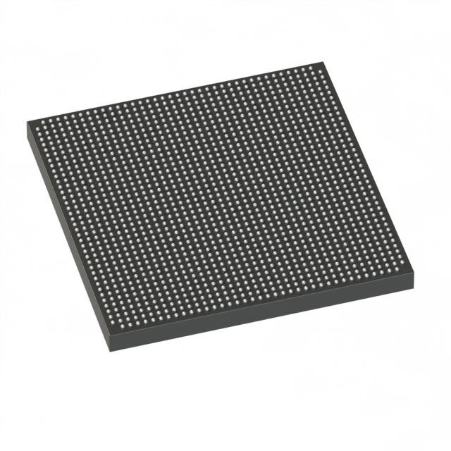
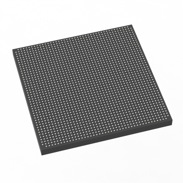
Stratix® V GX Field Programmable Gate Array (FPGA) IC 600 46080000 490000 1517-BBGA, FCBGA |
|---|---|
| Quantity | 812 Available (as of June 15, 2026) |

| Product Category | Field Programmable Gate Array (FPGA) |
|---|---|
| Manufacturer | Intel |
| Manufacturing Status | Obsolete |
| Manufacturer Standard Lead Time | Contact Us |
| Datasheet |
Specifications & Environmental
| Device Package | 1517-FBGA (40x40) | Grade | Commercial | Operating Temperature | 0°C – 85°C | ||
|---|---|---|---|---|---|---|---|
| Package / Case | 1517-BBGA, FCBGA | Number of I/O | 600 | Voltage | 820 mV - 880 mV | ||
| Mounting Method | Surface Mount | RoHS Compliance | RoHS Compliant | REACH Compliance | REACH Unknown | ||
| Moisture Sensitivity Level | 3 (168 Hours) | Number of LABs/CLBs | 185000 | Number of Logic Elements/Cells | 490000 | ||
| Number of Gates | N/A | ECCN | 3A001A2C | HTS Code | 8542.39.0001 | ||
| Qualification | N/A | Total RAM Bits | 46080000 |
Overview of 5SGXEA5N3F40C2LN – Stratix V GX FPGA, 490,000 logic elements
The 5SGXEA5N3F40C2LN is a Stratix® V GX field-programmable gate array (FPGA) IC from Intel, designed for high-density digital implementations. The device combines extensive logic resources, large on-chip memory, and a high I/O count to support complex system designs in communications, compute acceleration, and advanced signal processing.
With a core supply range of 820 mV to 880 mV and a commercial operating temperature range of 0 °C to 85 °C, this surface-mount FCBGA device is suited to commercial-grade applications requiring significant integration and high interconnect capacity.
Key Features
- Logic Capacity Approximately 490,000 logic elements (logic cells) to implement large, complex designs and multi-function systems.
- On-chip Memory Approximately 46.08 Mbits of embedded RAM (46,080,000 bits) for local storage, buffering, and state machine requirements.
- I/O Density 600 user I/O pins to support broad peripheral and high-pin-count interfacing requirements.
- Package 1517-BBGA FCBGA package (supplier package listed as 1517-FBGA, 40×40) for high-density board integration.
- Power Core voltage supply specified between 820 mV and 880 mV for the device core.
- Mounting & Grade Surface-mount device, commercial grade with an operating temperature range of 0 °C to 85 °C.
- Environmental RoHS compliant.
Typical Applications
- Networking and Communications High logic density and large I/O count enable complex packet processing, protocol bridging, and multi-port interfacing.
- Compute Acceleration On-chip RAM and abundant logic elements support custom acceleration blocks and data-path offload in compute systems.
- Signal Processing Large embedded memory and dense logic resources support DSP algorithms, real-time filtering, and data aggregation tasks.
Unique Advantages
- High integration density: 490,000 logic elements let you consolidate multiple functions into a single FPGA, reducing board complexity.
- Large embedded memory: Approximately 46.08 Mbits of on-chip RAM reduces reliance on external memory for buffering and state retention.
- Extensive I/O support: 600 I/Os provide flexibility for interfacing to numerous peripherals, high-speed PHYs, and complex mezzanine connections.
- Compact, manufacturable package: 1517-BBGA FCBGA (1517-FBGA, 40×40) enables dense PCB layouts while supporting surface-mount assembly.
- Commercial-grade operating range: Specified 0 °C to 85 °C operation and RoHS compliance for standard commercial deployments.
- Low-voltage core: 0.82–0.88 V supply range helps align power budgeting for modern low-voltage systems.
Why Choose 5SGXEA5N3F40C2LN?
The 5SGXEA5N3F40C2LN delivers a combination of substantial logic capacity, significant on-chip memory, and a high I/O count in a compact FCBGA package—making it well suited to commercial designs that demand integration and flexibility. As a member of the Stratix V GX family from Intel, it provides platform-level capabilities to implement complex data-paths, accelerators, and interface-rich systems.
For design teams targeting high-density FPGA implementations where on-chip RAM, logic resources, and I/O scalability are critical, this device provides a clear hardware foundation and predictable operating parameters for commercial deployments.
Request a quote or submit an inquiry for pricing and availability for the 5SGXEA5N3F40C2LN Stratix V GX FPGA.


Date Founded: 1968
Headquarters: Santa Clara, California, USA
Employees: 130,000+
Revenue: $54.23 Billion
Certifications and Memberships: ISO9001:2015, ISO14001:2015, ISO17025:2017, ISO27001:2022, ISO45001:2018, ISO50001:2018


