
5SGXEA5N3F45C2LN
| Part Description |
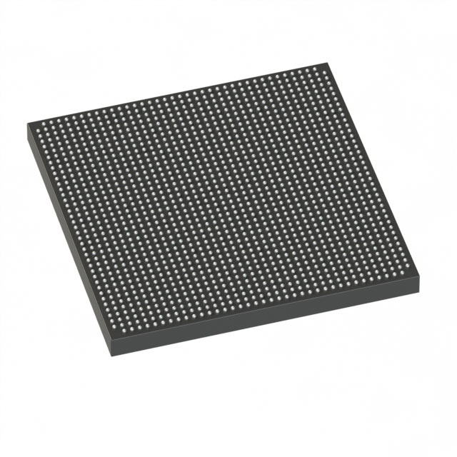
Stratix® V GX Field Programmable Gate Array (FPGA) IC 840 46080000 490000 1932-BBGA, FCBGA |
|---|---|
| Quantity | 1,471 Available (as of June 15, 2026) |

| Product Category | Field Programmable Gate Array (FPGA) |
|---|---|
| Manufacturer | Intel |
| Manufacturing Status | Obsolete |
| Manufacturer Standard Lead Time | Contact Us |
| Datasheet |
Specifications & Environmental
| Device Package | 1932-FBGA, FC (45x45) | Grade | Commercial | Operating Temperature | 0°C – 85°C | ||
|---|---|---|---|---|---|---|---|
| Package / Case | 1932-BBGA, FCBGA | Number of I/O | 840 | Voltage | 820 mV - 880 mV | ||
| Mounting Method | Surface Mount | RoHS Compliance | RoHS Compliant | REACH Compliance | REACH Unknown | ||
| Moisture Sensitivity Level | 3 (168 Hours) | Number of LABs/CLBs | 185000 | Number of Logic Elements/Cells | 490000 | ||
| Number of Gates | N/A | ECCN | 3A001A2C | HTS Code | 8542.39.0001 | ||
| Qualification | N/A | Total RAM Bits | 46080000 |
Overview of 5SGXEA5N3F45C2LN – Stratix® V GX Field Programmable Gate Array (FPGA) IC
The 5SGXEA5N3F45C2LN is a Stratix® V GX family FPGA in a 1932-ball FCBGA package designed for high-density, commercially graded applications. It combines a large logic fabric, substantial embedded memory, and a high I/O count to address complex digital designs where integration density and I/O capacity matter.
This device is commercial grade (0 °C to 85 °C), RoHS compliant, and operates at a core supply range of 820 mV to 880 mV. It is supplied in a surface-mount 1932-FBGA (45 × 45 mm) package.
Key Features
- Core Logic Approximately 490,000 logic elements, with around 185,000 logic array blocks for implementing large-scale digital logic and custom architectures.
- Embedded Memory Approximately 46.08 Mbits of on-chip RAM, providing substantial on-device buffering and storage for state machines, FIFOs, and algorithmic data.
- I/O Capacity Up to 840 I/O pins to support wide parallel interfaces, multi-channel connectivity, and complex board-level integration.
- Power Core voltage specified from 820 mV to 880 mV to match precise power domains and system-level power design.
- Package & Mounting 1932-ball BGA (FCBGA) surface-mount package, supplier package noted as 1932-FBGA, FC (45 × 45 mm) for high-density board designs.
- Operating Range & Compliance Commercial temperature grade (0 °C to 85 °C) and RoHS compliant for standard commercial product deployments.
- Series-Level Transceiver Information As a Stratix V GX family device, the series datasheet documents GX transceiver speed grades (series-level) used across the family.
Typical Applications
- High-performance Digital Processing Large logic capacity and embedded memory make this device suitable for compute-heavy FPGA tasks such as signal processing pipelines and real-time data manipulation.
- Communications & Networking High I/O counts and Stratix V GX family transceiver capabilities (series-level) support multi-channel interfaces and bandwidth-dense line cards.
- Instrumentation & Test Substantial on-chip RAM and abundant I/O enable complex data capture, buffering, and control functions in lab and production test equipment.
- Prototype & System Integration Dense logic and BGA packaging facilitate system-level prototyping and integration where board space and integration density are priorities.
Unique Advantages
- High Logic Density: Approximately 490,000 logic elements allow larger designs to be implemented in a single device, reducing multi‑device partitioning.
- Significant On‑Chip Memory: Around 46.08 Mbits of embedded RAM supports deep buffering and state retention without external memory overhead.
- Extensive I/O Resources: 840 I/O pins simplify interfacing to multiple peripherals and high-channel-count systems, lowering PCB routing complexity.
- Commercial Temperature & RoHS Compliance: Commercial temperature rating (0 °C to 85 °C) and RoHS compliance meet typical commercial deployment and environmental requirements.
- Compact High‑Density Package: 1932-ball FCBGA (45 × 45 mm) surface-mount package delivers high pin count in a compact footprint for dense system boards.
- Documented Series Support: Device is part of the Stratix V GX family with published device datasheet content for electrical characteristics and operating requirements.
Why Choose 5SGXEA5N3F45C2LN?
The 5SGXEA5N3F45C2LN positions itself as a high-density, commercially graded FPGA option in the Stratix V GX family for engineers who need extensive logic resources, on-chip memory, and a large I/O complement in a single, surface-mount BGA package. Its specified core voltage range and operating temperature make it suitable for a wide range of commercial electronic systems.
With detailed device documentation available for the Stratix V family, this FPGA is appropriate for teams building complex digital processing, communications, and instrumentation solutions that benefit from consolidated logic and memory resources on a single device.
Request a quote or submit an inquiry for pricing and availability to move your design forward with the 5SGXEA5N3F45C2LN.


Date Founded: 1968
Headquarters: Santa Clara, California, USA
Employees: 130,000+
Revenue: $54.23 Billion
Certifications and Memberships: ISO9001:2015, ISO14001:2015, ISO17025:2017, ISO27001:2022, ISO45001:2018, ISO50001:2018


