
5SGXEA7H2F35C2N
| Part Description |
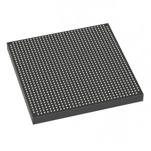
Stratix® V GX Field Programmable Gate Array (FPGA) IC 552 51200000 622000 1152-BBGA, FCBGA |
|---|---|
| Quantity | 949 Available (as of June 15, 2026) |

| Product Category | Field Programmable Gate Array (FPGA) |
|---|---|
| Manufacturer | Intel |
| Manufacturing Status | Obsolete |
| Manufacturer Standard Lead Time | Contact Us |
| Datasheet |
Specifications & Environmental
| Device Package | 1152-FBGA (35x35) | Grade | Commercial | Operating Temperature | 0°C – 85°C | ||
|---|---|---|---|---|---|---|---|
| Package / Case | 1152-BBGA, FCBGA | Number of I/O | 552 | Voltage | 870 mV - 930 mV | ||
| Mounting Method | Surface Mount | RoHS Compliance | RoHS Compliant | REACH Compliance | REACH Unknown | ||
| Moisture Sensitivity Level | 3 (168 Hours) | Number of LABs/CLBs | 234720 | Number of Logic Elements/Cells | 622000 | ||
| Number of Gates | N/A | ECCN | 3A001A2C | HTS Code | 8542.39.0001 | ||
| Qualification | N/A | Total RAM Bits | 51200000 |
Overview of 5SGXEA7H2F35C2N – Stratix V GX FPGA (622,000 logic elements)
The 5SGXEA7H2F35C2N is a Stratix® V GX field‑programmable gate array (FPGA) from Intel, offered as a commercial‑grade device. It delivers a high logic capacity FPGA fabric with a large on‑chip memory complement and extensive I/O, packaged in a 1152‑FBGA footprint for surface‑mount assembly.
Designed for demanding digital designs requiring significant programmable logic, embedded memory, and wide I/O counts, this device is suited to applications where high integration and design flexibility are priorities.
Key Features
- Logic Capacity Provides 622,000 logic elements for complex digital logic implementation and large FPGA designs.
- Embedded Memory Approximately 51.2 Mbits of on‑chip RAM to support large buffering, state storage, and memory‑intensive algorithms.
- I/O Density 552 device I/O pins to accommodate extensive external interfacing and high‑pin‑count connectivity.
- Package 1152‑BBGA / 1152‑FBGA (35x35) package case optimized for high‑density, surface‑mount system designs.
- Power Supply Core voltage supply range 870 mV to 930 mV to match system power domains and design requirements.
- Operating Range & Grade Commercial temperature grade with an operating temperature range of 0 °C to 85 °C.
- Mounting & Compliance Surface‑mount device; RoHS compliant for global environmental standards.
- Stratix V GX Family Characteristics Part of the Stratix V GX family; family datasheet documents commercial speed‑grade offerings and transceiver speed grade options for GX devices.
Typical Applications
- High‑performance digital signal processing Large logic capacity and abundant embedded memory enable implementation of complex DSP pipelines and algorithm acceleration.
- High‑density I/O bridging Extensive I/O count supports wide parallel interfaces, protocol bridging, and multi‑lane connectivity.
- Custom compute and hardware acceleration Significant logic resources and on‑chip RAM allow offloading compute‑intensive tasks from host processors.
Unique Advantages
- Large programmable fabric: 622,000 logic elements let designers map complex state machines, parallel datapaths, and large custom accelerators on a single device.
- Substantial embedded memory: Approximately 51.2 Mbits of on‑chip RAM reduces dependence on external memory for buffering and local storage, simplifying board design.
- High I/O availability: 552 I/O pins enable broad connectivity to sensors, interfaces, and mezzanine modules without signal multiplexing compromises.
- High‑density package: 1152‑FBGA (35x35) packaging supports compact board layouts while delivering the pin count required for complex systems.
- Commercial operating range: Rated for 0 °C to 85 °C operation to meet typical commercial and enterprise environmental requirements.
- Standards‑aware supply: RoHS compliance supports environmentally regulated product builds.
Why Choose 5SGXEA7H2F35C2N?
The 5SGXEA7H2F35C2N combines a large logic resource pool, substantial embedded memory, and a high I/O count in a compact 1152‑FBGA package, delivering a flexible platform for complex digital designs. As a commercial‑grade Stratix V GX device, it is positioned for engineering teams building high‑integration FPGA solutions that require significant on‑chip resources and broad connectivity.
This device is appropriate for customers focused on scalable FPGA implementations, where robust logic capacity, embedded memory, and system‑level I/O are primary selection criteria. The combination of package density, RoHS compliance, and defined commercial operating limits supports reliable integration into production systems.
Request a quote or submit a purchase inquiry to evaluate 5SGXEA7H2F35C2N for your next FPGA design project.


Date Founded: 1968
Headquarters: Santa Clara, California, USA
Employees: 130,000+
Revenue: $54.23 Billion
Certifications and Memberships: ISO9001:2015, ISO14001:2015, ISO17025:2017, ISO27001:2022, ISO45001:2018, ISO50001:2018


