
5SGXEA7H2F35C2W
| Part Description |
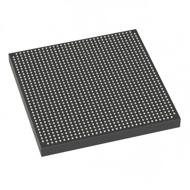
Stratix® V GX Field Programmable Gate Array (FPGA) IC 552 51200000 622000 1152-BBGA, FCBGA |
|---|---|
| Quantity | 1,483 Available (as of June 18, 2026) |

| Product Category | Field Programmable Gate Array (FPGA) |
|---|---|
| Manufacturer | Intel |
| Manufacturing Status | Obsolete |
| Manufacturer Standard Lead Time | Contact Us |
| Datasheet |
Specifications & Environmental
| Device Package | 1152-FBGA (35x35) | Grade | Commercial | Operating Temperature | 0°C – 85°C | ||
|---|---|---|---|---|---|---|---|
| Package / Case | 1152-BBGA, FCBGA | Number of I/O | 552 | Voltage | 870 mV - 930 mV | ||
| Mounting Method | Surface Mount | RoHS Compliance | RoHS Compliant | REACH Compliance | REACH Unknown | ||
| Moisture Sensitivity Level | 3 (168 Hours) | Number of LABs/CLBs | 234720 | Number of Logic Elements/Cells | 622000 | ||
| Number of Gates | N/A | ECCN | OBSOLETE | HTS Code | N/A | ||
| Qualification | N/A | Total RAM Bits | 51200000 |
Overview of 5SGXEA7H2F35C2W – Stratix® V GX Field Programmable Gate Array (FPGA) IC
The 5SGXEA7H2F35C2W is a Stratix V GX family field programmable gate array (FPGA) in a 1152-ball FCBGA package. It delivers high on-chip logic density, large embedded memory, and a broad I/O complement for demanding system designs.
Designed for commercial-temperature applications, this device combines 622,000 logic elements with approximately 51.2 Mbits of embedded memory and dedicated high-speed transceiver capability (per the Stratix V GX device datasheet), making it suitable for high-performance communications and complex signal-processing tasks.
Key Features
- Core Logic 622,000 logic elements provide substantial programmable fabric for complex designs and IP integration.
- Embedded Memory Approximately 51.2 Mbits of on-chip RAM to support large buffers, FIFOs, and memory-intensive algorithms.
- I/O and Transceivers 552 I/O pins for wide external connectivity; Stratix V GX transceiver speed grades are listed in the family datasheet (including GX channel rates such as 14.1 Gbps, 12.5 Gbps and 8.5 Gbps in specified speed grades).
- Power Tight core supply range of 870 mV to 930 mV supports predictable power budgeting and voltage planning.
- Package & Mounting 1152-ball BGA (1152-FBGA, 35×35) surface-mount package (FCBGA) for compact board-level integration.
- Operating Conditions Commercial temperature grade: 0 °C to 85 °C, suitable for a wide range of controlled-environment applications.
- Compliance RoHS-compliant construction supports modern regulatory requirements for electronic assemblies.
Typical Applications
- High‑speed communications Uses the Stratix V GX transceiver capability and abundant I/O to implement multi‑lane serial links and protocol bridging.
- Signal processing and acceleration Large logic capacity and significant on‑chip RAM support DSP pipelines, packet processing, and custom acceleration engines.
- System integration and prototyping High I/O count and a dense FCBGA package allow integration of complex interfaces and rapid hardware prototyping.
Unique Advantages
- High programmable density: 622,000 logic elements enable complex, multi‑function designs without immediate need for external logic.
- Substantial embedded memory: Approximately 51.2 Mbits of on‑chip RAM reduce dependence on external memory for buffering and state storage.
- Broad external connectivity: 552 I/Os provide flexible interfacing options for high-pin-count systems and mixed-signal front ends.
- High-speed serial support: Stratix V GX family transceiver speed grades (as documented in the device datasheet) support implementation of high-throughput serial links.
- Compact board footprint: 1152-ball FCBGA package delivers dense integration for space-constrained PCBs.
- RoHS-compliant: Supports current lead-free and environmental requirements for commercial electronic products.
Why Choose 5SGXEA7H2F35C2W?
The 5SGXEA7H2F35C2W positions itself as a high‑capacity, commercially graded Stratix V GX FPGA for applications that demand large programmable fabric, significant embedded memory, and substantial I/O. Its documented transceiver speed grades and high I/O count make it well suited to communications, signal processing, and system‑level integration projects where on‑chip resources and high throughput are priorities.
With a compact 1152-ball FCBGA package, defined core voltage range, and commercial operating temperature rating, this device offers a predictable platform for development cycles and production designs within controlled-environment markets.
Request a quote or submit a pricing inquiry to receive availability and purchasing information for the 5SGXEA7H2F35C2W.


Date Founded: 1968
Headquarters: Santa Clara, California, USA
Employees: 130,000+
Revenue: $54.23 Billion
Certifications and Memberships: ISO9001:2015, ISO14001:2015, ISO17025:2017, ISO27001:2022, ISO45001:2018, ISO50001:2018


