
5SGXEA7K1F40C2L
| Part Description |
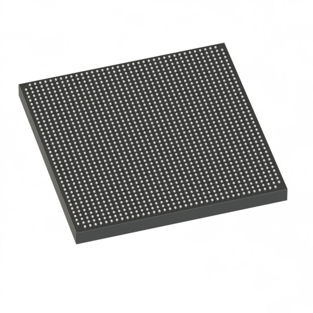
Stratix® V GX Field Programmable Gate Array (FPGA) IC 696 51200000 622000 1517-BBGA, FCBGA |
|---|---|
| Quantity | 665 Available (as of June 14, 2026) |

| Product Category | Field Programmable Gate Array (FPGA) |
|---|---|
| Manufacturer | Intel |
| Manufacturing Status | Obsolete |
| Manufacturer Standard Lead Time | Contact Us |
| Datasheet |
Specifications & Environmental
| Device Package | 1517-FBGA (40x40) | Grade | Commercial | Operating Temperature | 0°C – 85°C | ||
|---|---|---|---|---|---|---|---|
| Package / Case | 1517-BBGA, FCBGA | Number of I/O | 696 | Voltage | 820 mV - 880 mV | ||
| Mounting Method | Surface Mount | RoHS Compliance | RoHS Compliant | REACH Compliance | REACH Unknown | ||
| Moisture Sensitivity Level | 3 (168 Hours) | Number of LABs/CLBs | 234720 | Number of Logic Elements/Cells | 622000 | ||
| Number of Gates | N/A | ECCN | 3A001A2C | HTS Code | 8542.39.0001 | ||
| Qualification | N/A | Total RAM Bits | 51200000 |
Overview of 5SGXEA7K1F40C2L – Stratix® V GX FPGA, 1517-BBGA (FCBGA)
The Intel Stratix® V GX 5SGXEA7K1F40C2L is a high-capacity field programmable gate array (FPGA) in a 1517-BBGA FCBGA package. This commercial-grade Stratix V GX device provides substantial on-chip logic and memory with extensive I/O, suitable for designs that require high integration and flexible reprogrammability.
Designed within the Stratix V GX family, the device’s datasheet coverage includes transceiver specifications, core and periphery switching characteristics, and I/O timing, making it appropriate for engineering projects that demand detailed electrical and timing control during system design.
Key Features
- Logic Capacity Provides 622,000 logic elements to implement large-scale digital logic and custom architectures.
- Embedded Memory Approximately 51.2 Mbits of on-chip RAM for buffering, LUT-based storage, and intermediate data processing.
- I/O Resources 696 device I/Os to support wide parallel interfaces and extensive external connectivity.
- Transceiver and I/O Timing Datasheet includes transceiver specifications and programmable I/O element timing for precise interface design and signal integrity planning.
- Power Core supply voltage range: 820 mV to 880 mV, enabling designs that target low-voltage core rails.
- Package & Mounting 1517-BBGA (FCBGA) package; supplier package listed as 1517-FBGA (40×40). Surface-mount device suitable for standard PCB assembly processes.
- Operating Grade & Temperature Commercial grade device rated for 0 °C to 85 °C operation.
- Compliance RoHS-compliant for environmentally conscious designs.
Typical Applications
- High-density digital systems Implement large programmable logic blocks and complex state machines using the device’s extensive logic element count.
- Memory-intensive designs Leverage approximately 51.2 Mbits of embedded RAM for buffering, packet processing, and on-chip data storage.
- Wide-interface systems Support broad external connectivity and parallel data paths with 696 I/Os.
Unique Advantages
- High logic integration: 622,000 logic elements enable consolidation of multiple functions into a single FPGA, reducing board-level component count.
- Significant on-chip memory: Approximately 51.2 Mbits of embedded RAM supports data-heavy tasks without immediate external memory dependence.
- Extensive I/O availability: 696 I/Os provide flexibility for interfacing to multiple peripherals, buses, and parallel channels.
- Compact, production-ready package: 1517-BBGA FCBGA (1517-FBGA 40×40) surface-mount package for space-efficient PCB implementations.
- Low-voltage core operation: Core supply range of 820–880 mV aligns with low-voltage power architectures.
- Environmental compliance: RoHS status supports regulatory and sustainability requirements.
Why Choose 5SGXEA7K1F40C2L?
The 5SGXEA7K1F40C2L combines large logic capacity, substantial embedded memory, and a high I/O count within a compact FCBGA package, offering a highly integrated solution for commercial-grade FPGA designs. Its documented transceiver and I/O timing characteristics, along with defined electrical operating conditions, support detailed system integration and timing validation.
This part is well suited for engineers and procurement teams building complex digital systems that require on-chip resources for logic and memory, broad external interfacing, and a commercial temperature grade. Choosing this Stratix V GX device provides a verified platform with clear electrical and packaging specifications for production designs.
Request a quote or submit an RFQ to receive pricing and availability information for the 5SGXEA7K1F40C2L. Provide your quantity and delivery requirements to expedite the response.


Date Founded: 1968
Headquarters: Santa Clara, California, USA
Employees: 130,000+
Revenue: $54.23 Billion
Certifications and Memberships: ISO9001:2015, ISO14001:2015, ISO17025:2017, ISO27001:2022, ISO45001:2018, ISO50001:2018


