
5SGXEA7K2F40C3N
| Part Description |
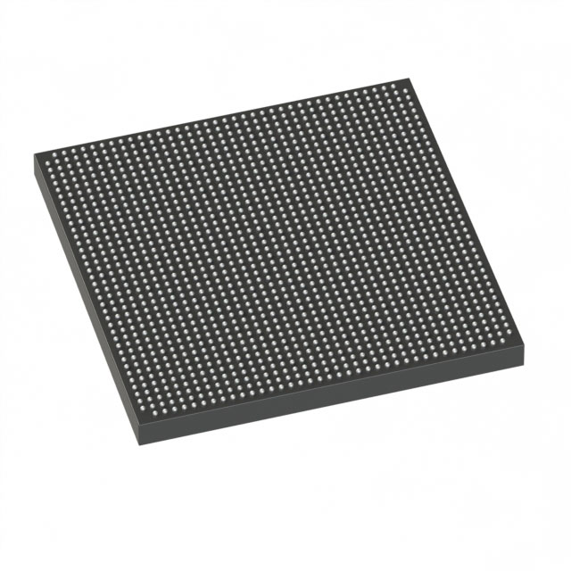
Stratix® V GX Field Programmable Gate Array (FPGA) IC 696 51200000 622000 1517-BBGA, FCBGA |
|---|---|
| Quantity | 103 Available (as of June 15, 2026) |

| Product Category | Field Programmable Gate Array (FPGA) |
|---|---|
| Manufacturer | Intel |
| Manufacturing Status | Obsolete |
| Manufacturer Standard Lead Time | Contact Us |
| Datasheet |
Specifications & Environmental
| Device Package | 1517-FBGA (40x40) | Grade | Commercial | Operating Temperature | 0°C – 85°C | ||
|---|---|---|---|---|---|---|---|
| Package / Case | 1517-BBGA, FCBGA | Number of I/O | 696 | Voltage | 820 mV - 880 mV | ||
| Mounting Method | Surface Mount | RoHS Compliance | RoHS Compliant | REACH Compliance | REACH Unknown | ||
| Moisture Sensitivity Level | 3 (168 Hours) | Number of LABs/CLBs | 234720 | Number of Logic Elements/Cells | 622000 | ||
| Number of Gates | N/A | ECCN | 3A001A2C | HTS Code | 8542.39.0001 | ||
| Qualification | N/A | Total RAM Bits | 51200000 |
Overview of 5SGXEA7K2F40C3N – Stratix® V GX FPGA, 622,000 logic elements, 1517-BBGA
The 5SGXEA7K2F40C3N is a Stratix® V GX field programmable gate array (FPGA) IC from Intel. It provides a high-density programmable fabric with large embedded memory and extensive I/O in a surface-mount FCBGA package.
Designed for designs that require significant logic capacity, on-chip RAM, and high-speed transceiver capability available in the Stratix V GX family, this commercial-grade device supports core voltages from 820 mV to 880 mV and operates across a commercial temperature range of 0 °C to 85 °C.
Key Features
- Core logic density — 622,000 logic elements to implement complex digital systems and large-scale programmable logic.
- Embedded memory — Approximately 51.2 Mbits of on-chip RAM for buffering, storage, and algorithm acceleration without external memory.
- I/O and package — 696 user I/Os in a 1517-BBGA (FCBGA) package; surface-mount mounting simplifies board-level integration. Supplier device package: 1517-FBGA (40×40).
- Stratix V GX transceiver capability — Device belongs to the Stratix V GX family; the family datasheet documents GX channel transceiver grades (including channels up to 14.1 Gbps for the GX family) for high-speed serial connectivity.
- Power supply — Core voltage range from 820 mV to 880 mV to match system power rails and design constraints.
- Commercial operating range — Rated for 0 °C to 85 °C operating temperature; commercial grade device.
- Compliance — RoHS compliant.
Typical Applications
- High-speed serial connectivity — Designs that leverage Stratix V GX transceivers for protocol bridging and high-bandwidth links.
- Complex digital systems — Implement large-scale state machines, datapaths, and custom hardware accelerators using the device’s high logic element count and embedded RAM.
- Deterministic I/O timing designs — Systems requiring precise I/O timing and periphery performance documented in the Stratix V device datasheet.
Unique Advantages
- High integration density: 622,000 logic elements and ~51.2 Mbits of embedded memory reduce the need for external components and simplify system architecture.
- Extensive I/O availability: 696 I/Os in a compact FCBGA footprint enable rich peripheral connectivity and multi-channel interfaces without additional I/O expanders.
- Family-level transceiver support: As a Stratix V GX device, it aligns with family transceiver specifications for high-speed serial channels, supporting designs that require high bandwidth links.
- Commercial temperature and RoHS compliance: Specified for 0 °C to 85 °C operation and RoHS compliant for standard commercial deployments.
- Surface-mount FCBGA package: The 1517-BBGA package and 1517-FBGA (40×40) supplier package enable dense PCB implementations suitable for advanced system boards.
Why Choose 5SGXEA7K2F40C3N?
The 5SGXEA7K2F40C3N provides a high-capacity Stratix V GX FPGA option for engineers building complex, high-performance digital systems that require substantial on-chip logic and memory alongside family-level transceiver capabilities. Its large I/O count and compact FCBGA package make it suitable for dense board designs where integration and predictable I/O timing matter.
Backed by Intel’s Stratix V device documentation, this commercial-grade FPGA offers a vetted platform for scalable designs that need programmable flexibility, embedded RAM, and the Stratix V GX transceiver feature set.
Request a quote or submit an inquiry to receive pricing and availability information for the 5SGXEA7K2F40C3N.


Date Founded: 1968
Headquarters: Santa Clara, California, USA
Employees: 130,000+
Revenue: $54.23 Billion
Certifications and Memberships: ISO9001:2015, ISO14001:2015, ISO17025:2017, ISO27001:2022, ISO45001:2018, ISO50001:2018


