
5SGXEA7N2F45C1G
| Part Description |
Stratix® V GX Field Programmable Gate Array (FPGA) IC 840 51200000 622000 1932-BBGA, FCBGA |
|---|---|
| Quantity | 857 Available (as of June 16, 2026) |

| Product Category | Field Programmable Gate Array (FPGA) |
|---|---|
| Manufacturer | Intel |
| Manufacturing Status | Active |
| Manufacturer Standard Lead Time | 26 Weeks |
| Datasheet |
Specifications & Environmental
| Device Package | 1932-FBGA, FC (45x45) | Grade | Commercial | Operating Temperature | 0°C – 85°C | ||
|---|---|---|---|---|---|---|---|
| Package / Case | 1932-BBGA, FCBGA | Number of I/O | 840 | Voltage | 870 mV - 930 mV | ||
| Mounting Method | Surface Mount | RoHS Compliance | RoHS Compliant | REACH Compliance | REACH Unaffected | ||
| Moisture Sensitivity Level | 3 (168 Hours) | Number of LABs/CLBs | 234720 | Number of Logic Elements/Cells | 622000 | ||
| Number of Gates | N/A | ECCN | N/A | HTS Code | N/A | ||
| Qualification | N/A | Total RAM Bits | 51200000 |
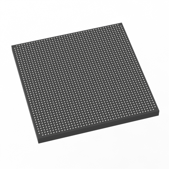
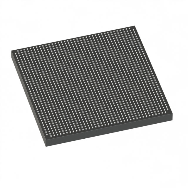
Overview of 5SGXEA7N2F45C1G – Stratix® V GX FPGA (Commercial, 1932-BBGA)
The 5SGXEA7N2F45C1G is a Stratix® V GX Field Programmable Gate Array (FPGA) from Intel, provided in a 1932-ball FCBGA package for surface-mount assembly. It delivers very large programmable logic capacity and embedded memory with a broad set of I/O resources in a commercial-grade device.
Designed for designs that require high logic density, substantial on-chip RAM and extensive I/O, this device combines 622,000 logic elements with approximately 51.2 Mbits of embedded memory and up to 840 I/O pins while operating within a core voltage range of 870 mV to 930 mV and a commercial temperature range of 0 °C to 85 °C.
Key Features
- Core Logic 622,000 logic elements provide large-scale programmable logic capacity for complex digital designs and high-density implementations.
- Embedded Memory Approximately 51.2 Mbits of on-chip RAM for buffering, data storage, and high-throughput algorithm implementation.
- I/O Capacity Up to 840 user I/O pins to accommodate wide parallel interfaces, large bus structures, and multiple peripheral connections.
- Power and Supply Core supply range of 870 mV to 930 mV to match system power rails and enable predictable core performance within specified limits.
- Package and Mounting 1932-ball BGA (FCBGA, supplier package 1932-FBGA, FC 45×45) in a surface-mount form factor for compact board-level integration.
- Commercial Grade Operation Rated for commercial temperature operation from 0 °C to 85 °C.
- RoHS Compliance Device is RoHS compliant for global electronics manufacturing requirements.
Typical Applications
- High-density digital processing — Leverage 622,000 logic elements and extensive embedded RAM for large-scale FPGA-implemented algorithms and custom accelerators.
- Multi-channel I/O systems — Use up to 840 I/Os to interface with wide parallel buses, multi-lane data paths, or numerous peripherals.
- Memory-intensive designs — Approximately 51.2 Mbits of on-chip RAM supports buffering, packet processing, or storage for real-time data flows.
Unique Advantages
- High logic density: 622,000 logic elements enable consolidation of complex functions into a single FPGA, reducing board-level integration complexity.
- Substantial on-chip memory: Approximately 51.2 Mbits of embedded RAM minimizes external memory dependence for many data-path and buffering needs.
- Extensive I/O resources: 840 I/Os provide flexibility for diverse interface requirements and parallel connectivity without immediate need for I/O expanders.
- Compact package: 1932-ball FCBGA in a 45×45 outline supports high integration density in space-constrained PCB designs.
- Commercial temperature rating: Specified operation from 0 °C to 85 °C for standard commercial deployments.
Why Choose 5SGXEA7N2F45C1G?
The 5SGXEA7N2F45C1G combines very large programmable logic resources, significant on-chip RAM, and broad I/O capability in a compact FCBGA package, making it suited to high-density, memory-intensive, and I/O-rich FPGA applications that operate within commercial temperature ranges. As a Stratix® V GX device from Intel, it aligns with system designs that demand consolidated logic and memory on a single programmable device while retaining predictable electrical and thermal operating ranges.
This part is appropriate for engineering teams and procurement focused on high-capacity FPGA implementations where integration density, embedded memory, and extensive I/O are primary selection criteria.
Request a quote or submit a purchase inquiry for part number 5SGXEA7N2F45C1G to receive pricing and availability details.


Date Founded: 1968
Headquarters: Santa Clara, California, USA
Employees: 130,000+
Revenue: $54.23 Billion
Certifications and Memberships: ISO9001:2015, ISO14001:2015, ISO17025:2017, ISO27001:2022, ISO45001:2018, ISO50001:2018


