
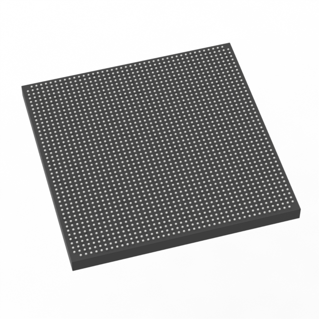
5SGXEA7N2F45C1WN
| Part Description |
Stratix® V GX Field Programmable Gate Array (FPGA) IC 840 51200000 622000 1932-BBGA, FCBGA |
|---|---|
| Quantity | 1,147 Available (as of October 7, 2026) |
| Product Category | Field Programmable Gate Array (FPGA) |
|---|---|
| Manufacturer | Intel |
| Manufacturing Status | Obsolete |
| Manufacturer Standard Lead Time | Contact Us |
| Datasheet |
Specifications & Environmental
| Device Package | 1932-FBGA, FC (45x45) | Grade | Commercial | Operating Temperature | 0°C – 85°C | ||
|---|---|---|---|---|---|---|---|
| Package / Case | 1932-BBGA, FCBGA | Number of I/O | 840 | Voltage | 870 mV - 930 mV | ||
| Mounting Method | Surface Mount | RoHS Compliance | RoHS non-compliant | REACH Compliance | REACH Unknown | ||
| Moisture Sensitivity Level | 4 (72 Hours) | Number of LABs/CLBs | 234720 | Number of Logic Elements/Cells | 622000 | ||
| Number of Gates | N/A | ECCN | OBSOLETE | HTS Code | N/A | ||
| Qualification | N/A | Total RAM Bits | 51200000 |
Overview of 5SGXEA7N2F45C1WN – Stratix® V GX Field Programmable Gate Array (FPGA), 1932‑BBGA
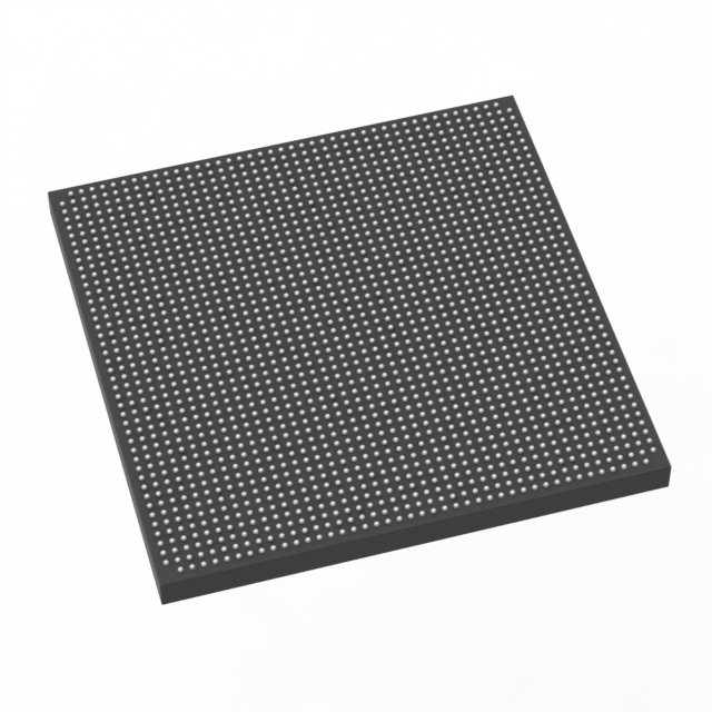
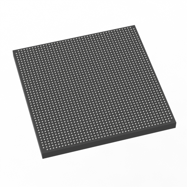
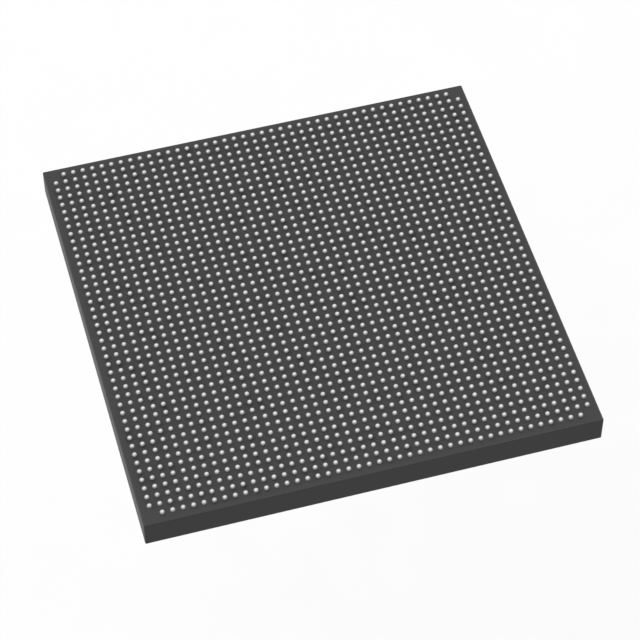
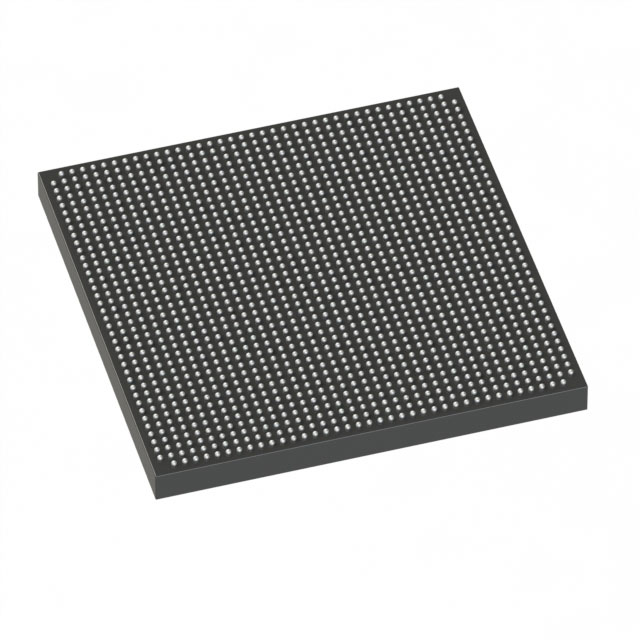
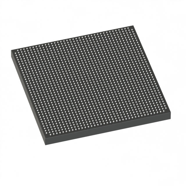
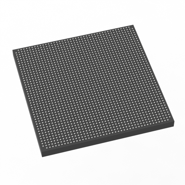
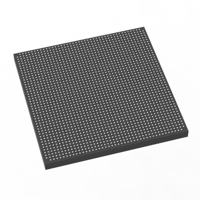
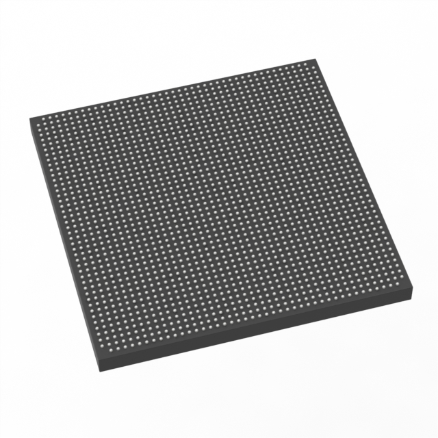
The 5SGXEA7N2F45C1WN is a Stratix V GX family field‑programmable gate array (FPGA) IC from Intel, delivered in a 1932‑ball FCBGA package. It provides a high‑density programmable fabric with substantial embedded memory and a large I/O count for complex digital designs.
With hundreds of thousands of logic resources, tens of megabits of on‑chip RAM and an industry‑standard surface‑mount BGA package, this commercial‑grade device targets designs that require large programmable logic capacity, significant on‑chip memory and extensive I/O connectivity.
Key Features
- Core & Logic 622,000 logic element cells and 234,720 LABs/CLBs provide extensive programmable logic capacity for complex state machines, datapaths and control logic.
- Embedded Memory Approximately 51.2 Mbits of on‑chip RAM for buffering, FIFOs, lookup tables and other memory‑intensive functions.
- I/O Density 840 I/O pins enable wide parallel interfaces and extensive external connectivity in a single device.
- Package & Mounting 1932‑BBGA FCBGA (1932‑FBGA, FC 45×45) in a surface‑mount form factor for compact, high‑pin‑count board designs.
- Power Core supply range specified from 870 mV to 930 mV, supporting the device’s power requirements within defined operating conditions.
- Temperature & Grade Commercial grade operation with an operating temperature range of 0 °C to 85 °C.
- Environmental Compliance RoHS compliant.
Typical Applications
- High‑density digital systems Use the large pool of logic elements and embedded memory for complex control, data‑path and signal processing implementations.
- Multi‑interface controllers Leverage 840 I/Os to consolidate numerous parallel and serial interfaces on a single FPGA for system integration.
- Prototyping and system validation Deploy the device for hardware prototyping where abundant programmable resources and on‑chip RAM are required.
Unique Advantages
- Extensive programmable capacity: Hundreds of thousands of logic element cells enable large, complex designs without partitioning across multiple FPGAs.
- Substantial on‑chip memory: Approximately 51.2 Mbits of embedded RAM reduces dependence on external memory for buffering and temporary storage.
- High I/O count: 840 I/Os simplify board‑level routing and enable direct interfacing to many peripherals and subsystems.
- Compact, high‑pin package: The 1932‑BBGA FCBGA package delivers high connectivity in a 45 × 45 mm footprint suitable for dense PCBs.
- Commercial temperature grade: Specified operation from 0 °C to 85 °C for standard commercial applications.
- RoHS compliance: Meets common environmental requirements for lead‑free assemblies.
Why Choose 5SGXEA7N2F45C1WN?
The 5SGXEA7N2F45C1WN combines large programmable logic resources, significant embedded memory and a very high I/O count in a single commercial‑grade Stratix V GX package. It is well suited to engineers designing complex digital systems that need to minimize board count while maximizing on‑chip capability.
For teams focused on scalability and integration, this FPGA offers a balance of dense logic, ample RAM and compact packaging that supports sophisticated system‑level designs and prototyping efforts, backed by Intel’s Stratix V device family documentation.
Request a quote or submit a procurement inquiry to receive pricing, lead‑time and availability information for the 5SGXEA7N2F45C1WN.





















Date Founded: 1968
Headquarters: Santa Clara, California, USA
Employees: 130,000+
Revenue: $54.23 Billion
Certifications and Memberships: ISO9001:2015, ISO14001:2015, ISO17025:2017, ISO27001:2022, ISO45001:2018, ISO50001:2018


