
5SGXEA7N2F45I3N
| Part Description |
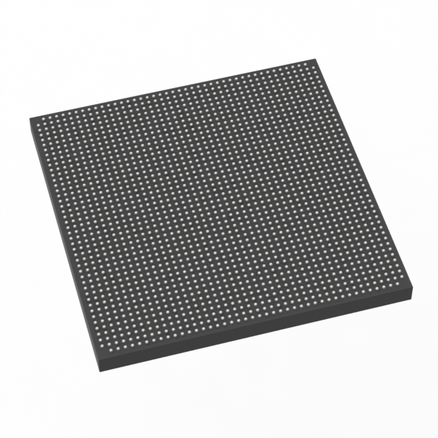
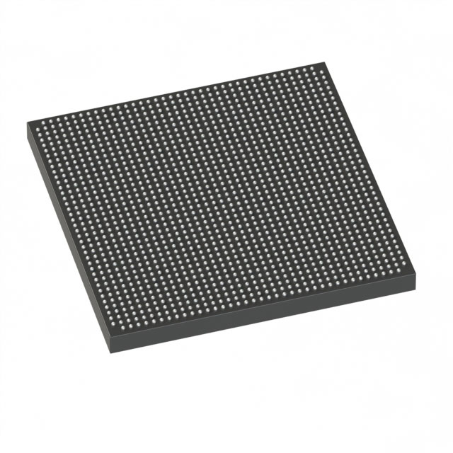
Stratix® V GX Field Programmable Gate Array (FPGA) IC 840 51200000 622000 1932-BBGA, FCBGA |
|---|---|
| Quantity | 1,436 Available (as of June 14, 2026) |

| Product Category | Field Programmable Gate Array (FPGA) |
|---|---|
| Manufacturer | Intel |
| Manufacturing Status | Obsolete |
| Manufacturer Standard Lead Time | Contact Us |
| Datasheet |
Specifications & Environmental
| Device Package | 1932-FBGA, FC (45x45) | Grade | Industrial | Operating Temperature | -40°C – 100°C | ||
|---|---|---|---|---|---|---|---|
| Package / Case | 1932-BBGA, FCBGA | Number of I/O | 840 | Voltage | 820 mV - 880 mV | ||
| Mounting Method | Surface Mount | RoHS Compliance | RoHS Compliant | REACH Compliance | REACH Unknown | ||
| Moisture Sensitivity Level | 3 (168 Hours) | Number of LABs/CLBs | 234720 | Number of Logic Elements/Cells | 622000 | ||
| Number of Gates | N/A | ECCN | 3A001A2C | HTS Code | 8542.39.0001 | ||
| Qualification | N/A | Total RAM Bits | 51200000 |
Overview of 5SGXEA7N2F45I3N – Stratix® V GX FPGA, 840 I/O, 1932-BBGA
The 5SGXEA7N2F45I3N is a Stratix® V GX Field Programmable Gate Array (FPGA) IC from Intel, supplied in a 1932-ball FBGA (FCBGA) package. This device delivers a large programmable fabric with dedicated embedded memory and extensive I/O for designs that require high logic density and advanced serial I/O capability within an industrial temperature grade.
Key on-chip resources include 622,000 logic elements and approximately 51.2 Mbits of embedded RAM, combined with 840 user I/O pins and GX-class transceiver support as documented for the Stratix V GX family. The device is specified for industrial operation and RoHS compliant.
Key Features
- Programmable Logic — 622,000 logic elements provide a substantial programmable fabric for complex digital designs and high-density logic implementation.
- Embedded Memory — Approximately 51.2 Mbits of on-chip RAM to support buffering, local data storage, and memory-intensive processing functions.
- High I/O Count — 840 user I/O pins enable broad connectivity for parallel interfaces, control signals, and board-level integration.
- GX Transceiver Capability — As part of the Stratix V GX family, GX channel transceivers are supported (Stratix V GX device datasheet lists GX channel speeds up to 14.1 Gbps), enabling high-speed serial links where required.
- Power — Core supply specified between 820 mV and 880 mV to match Stratix V core voltage requirements.
- Package & Mounting — 1932-ball BGA (FCBGA) package, supplier device package listed as 1932-FBGA, FC (45×45); surface-mount mounting type for standard board assembly.
- Industrial Temperature Grade — Rated for operation from −40 °C to 100 °C for deployments in industrial environments.
- Standards Compliance — RoHS compliant to support regulatory requirements for lead-free assembly.
Typical Applications
- High-density digital processing — Large logic capacity (622,000 logic elements) and substantial embedded RAM support complex algorithm implementation and parallel processing pipelines.
- High-speed serial communications — GX transceiver capability in the Stratix V GX family (documented up to 14.1 Gbps) suits designs requiring multi‑Gbps serial links and backplane connectivity.
- Industrial control and instrumentation — Industrial temperature grade (−40 °C to 100 °C) and high I/O count (840) enable robust I/O interfacing and control system integration.
Unique Advantages
- Large programmable fabric: 622,000 logic elements enable consolidation of multiple functions into a single device, reducing board-level component count.
- Substantial on-chip memory: Approximately 51.2 Mbits of embedded RAM reduces external memory dependence for buffering and local data storage.
- Extensive I/O flexibility: 840 user I/Os provide flexibility for mixed parallel and serial interfaces across complex designs.
- Industrial-rated operation: −40 °C to 100 °C operating range supports deployment in a wide range of industrial environments.
- Package density: 1932-ball FCBGA (45×45) package offers a compact, surface-mount solution for high-pin-count FPGA deployment.
- Regulatory readiness: RoHS compliance facilitates lead-free manufacturing and global environmental requirements.
Why Choose 5SGXEA7N2F45I3N?
The 5SGXEA7N2F45I3N Stratix® V GX FPGA combines a very large logic fabric, substantial embedded memory, and a high pin count in a 1932‑ball FCBGA package engineered for industrial temperature operation. These attributes make it suitable for designs that require dense logic integration, on-chip buffering, and extensive I/O or high-speed serial links.
For engineering teams targeting scalable, high‑density FPGA solutions within Intel’s Stratix V GX family, this part provides a verifiable set of resources and environmental ratings that support long-term deployments and complex system integration.
Request a quote or submit an inquiry to receive pricing and availability information for part number 5SGXEA7N2F45I3N.


Date Founded: 1968
Headquarters: Santa Clara, California, USA
Employees: 130,000+
Revenue: $54.23 Billion
Certifications and Memberships: ISO9001:2015, ISO14001:2015, ISO17025:2017, ISO27001:2022, ISO45001:2018, ISO50001:2018


