
5SGXEA7N2F45I3WN
| Part Description |
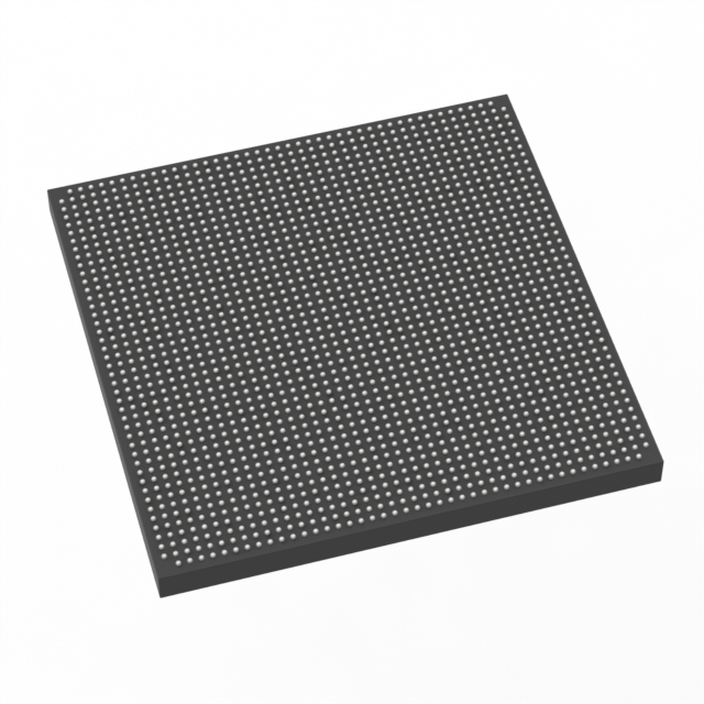
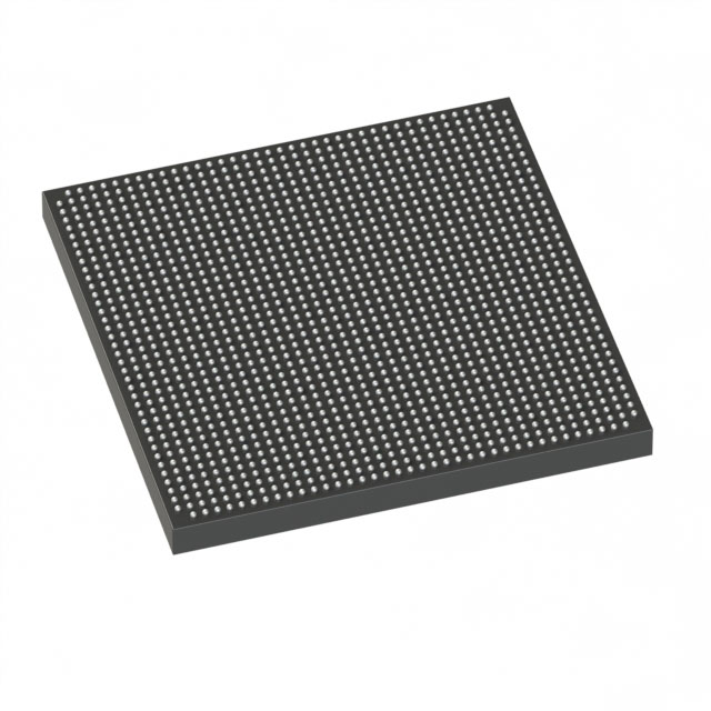
Stratix® V GX Field Programmable Gate Array (FPGA) IC 840 51200000 622000 1932-BBGA, FCBGA |
|---|---|
| Quantity | 769 Available (as of June 15, 2026) |

| Product Category | Field Programmable Gate Array (FPGA) |
|---|---|
| Manufacturer | Intel |
| Manufacturing Status | Obsolete |
| Manufacturer Standard Lead Time | Contact Us |
| Datasheet |
Specifications & Environmental
| Device Package | 1932-FBGA, FC (45x45) | Grade | Industrial | Operating Temperature | -40°C – 100°C | ||
|---|---|---|---|---|---|---|---|
| Package / Case | 1932-BBGA, FCBGA | Number of I/O | 840 | Voltage | 820 mV - 880 mV | ||
| Mounting Method | Surface Mount | RoHS Compliance | RoHS non-compliant | REACH Compliance | REACH Unknown | ||
| Moisture Sensitivity Level | 4 (72 Hours) | Number of LABs/CLBs | 234720 | Number of Logic Elements/Cells | 622000 | ||
| Number of Gates | N/A | ECCN | OBSOLETE | HTS Code | N/A | ||
| Qualification | N/A | Total RAM Bits | 51200000 |
Overview of 5SGXEA7N2F45I3WN – Stratix® V GX Field Programmable Gate Array (FPGA) IC
The 5SGXEA7N2F45I3WN is a Stratix® V GX Field Programmable Gate Array (FPGA) IC designed for high-density, transceiver-enabled digital designs. It combines a large logic fabric, substantial embedded memory, and a high I/O count to support complex, high-performance implementations.
As a member of the Stratix V GX family, the part is positioned for applications that require extensive programmable logic, numerous I/O, and series transceiver capabilities defined in the Stratix V GX device datasheet. The device is provided in an industrial temperature grade and packaged for surface-mount assembly.
Key Features
- Core Logic 622,000 logic elements provide a high-density programmable fabric for complex digital logic integration.
- Embedded Memory Approximately 51.2 Mbits of on-chip RAM to support buffers, state storage, and large FPGA designs.
- I/O Capacity 840 user I/O pins to interface with a wide range of external devices and peripherals.
- Transceiver Family Capability As part of the Stratix V GX series, transceiver speed grades in the family include rates up to 14.1 Gbps as documented in the device datasheet.
- Power Specified operating voltage supply range of 820 mV to 880 mV for the device core.
- Package & Mounting 1932-BBGA, FCBGA package case; supplier device package listed as 1932-FBGA, FC (45x45). Surface-mount mounting type.
- Temperature & Grade Industrial grade with an operating temperature range of −40°C to 100°C for deployment in temperature-demanding environments.
- Regulatory RoHS compliant.
Typical Applications
- High-speed communications — Implement transceiver-enabled links and protocol processing where family transceiver speed grades are required.
- Data processing and acceleration — Leverage the large logic element count and on-chip memory for compute- and buffer-intensive acceleration tasks.
- Instrumentation and test equipment — Use the high I/O count and dense logic resources for complex measurement, capture, and control functions.
- Industrial control systems — Industrial temperature rating and robust packaging make the device suitable for demanding control and automation applications.
Unique Advantages
- High logic density: 622,000 logic elements allow consolidation of large functions into a single device, reducing system complexity.
- Significant on-chip memory: Approximately 51.2 Mbits of embedded RAM provide ample storage for buffers, FIFOs, and working memory without external DRAM.
- Extensive I/O support: 840 I/Os enable broad peripheral and board-level interfacing without multiple devices.
- Industrial temperature range: Rated from −40°C to 100°C to meet demanding environmental requirements.
- Surface-mount, high-pin-count package: 1932-BBGA/1932-FBGA packaging supports high-density board designs while maintaining manufacturability.
- Series-level transceiver capability: Family transceiver speed grades documented in the datasheet support high-bandwidth serial links where needed.
Why Choose 5SGXEA7N2F45I3WN?
The 5SGXEA7N2F45I3WN delivers a combination of high logic capacity, substantial embedded memory, and a very large I/O complement in a surface-mount, industrial-grade FPGA package. These characteristics make it a strong choice for developers building complex, high-performance digital systems that require consolidation of functions, robust interfacing, and series transceiver capability at the device-family level.
For designs where scalability, thermal robustness, and a dense programmable fabric matter, this Stratix V GX device provides the resources to implement large-scale logic, buffering, and I/O requirements while remaining compliant with industry environmental standards.
Request a quote or submit your pricing request to obtain availability and ordering information for part number 5SGXEA7N2F45I3WN.


Date Founded: 1968
Headquarters: Santa Clara, California, USA
Employees: 130,000+
Revenue: $54.23 Billion
Certifications and Memberships: ISO9001:2015, ISO14001:2015, ISO17025:2017, ISO27001:2022, ISO45001:2018, ISO50001:2018


