
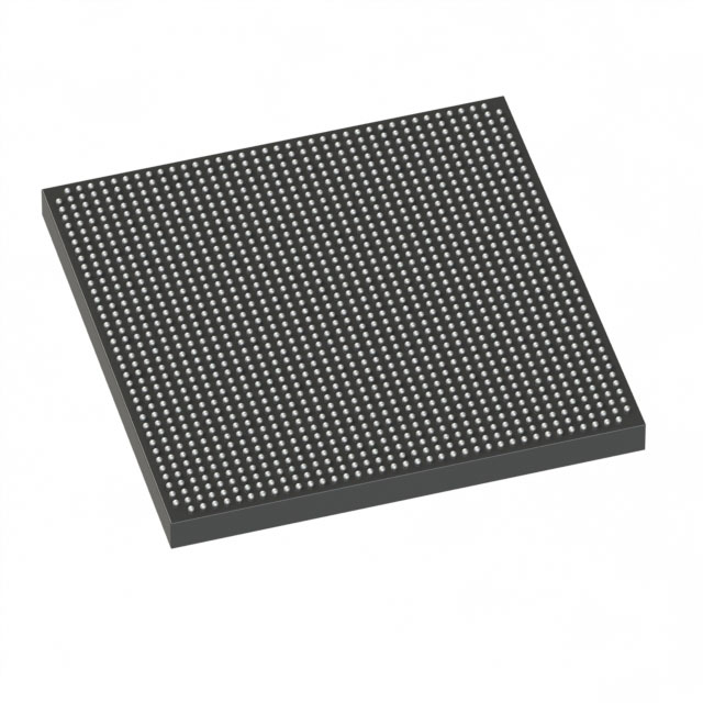
5SGXEABK2H40C2G
| Part Description |
Stratix® V GX Field Programmable Gate Array (FPGA) IC 696 53248000 952000 1517-BBGA, FCBGA |
|---|---|
| Quantity | 1,288 Available (as of October 7, 2026) |
| Product Category | Field Programmable Gate Array (FPGA) |
|---|---|
| Manufacturer | Intel |
| Manufacturing Status | Active |
| Manufacturer Standard Lead Time | 26 Weeks |
| Datasheet |
Specifications & Environmental
| Device Package | 1517-HBGA (45x45) | Grade | Commercial | Operating Temperature | 0°C – 85°C | ||
|---|---|---|---|---|---|---|---|
| Package / Case | 1517-BBGA, FCBGA | Number of I/O | 696 | Voltage | 870 mV - 930 mV | ||
| Mounting Method | Surface Mount | RoHS Compliance | RoHS Compliant | REACH Compliance | REACH Unaffected | ||
| Moisture Sensitivity Level | 3 (168 Hours) | Number of LABs/CLBs | 359200 | Number of Logic Elements/Cells | 952000 | ||
| Number of Gates | N/A | ECCN | N/A | HTS Code | N/A | ||
| Qualification | N/A | Total RAM Bits | 53248000 |
Overview of 5SGXEABK2H40C2G – Stratix® V GX Field Programmable Gate Array (FPGA) IC, 1517-BBGA
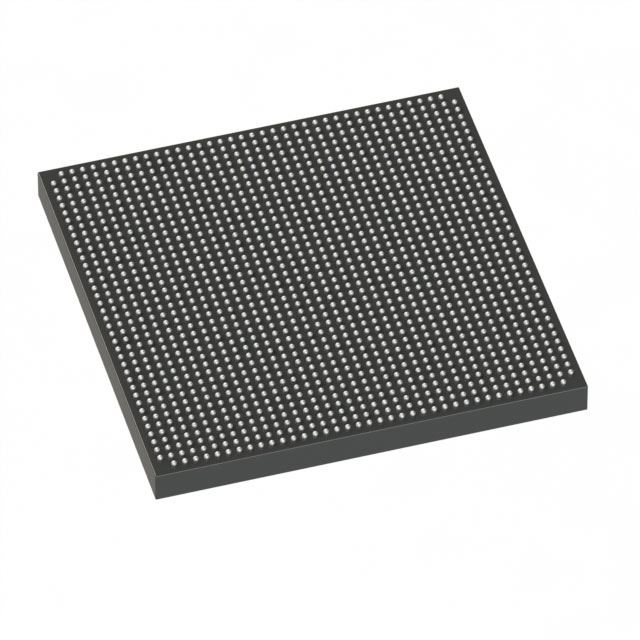
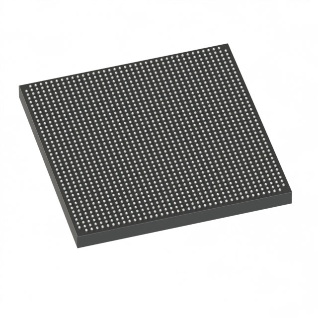
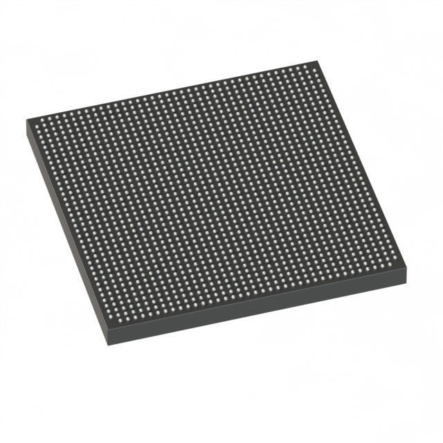
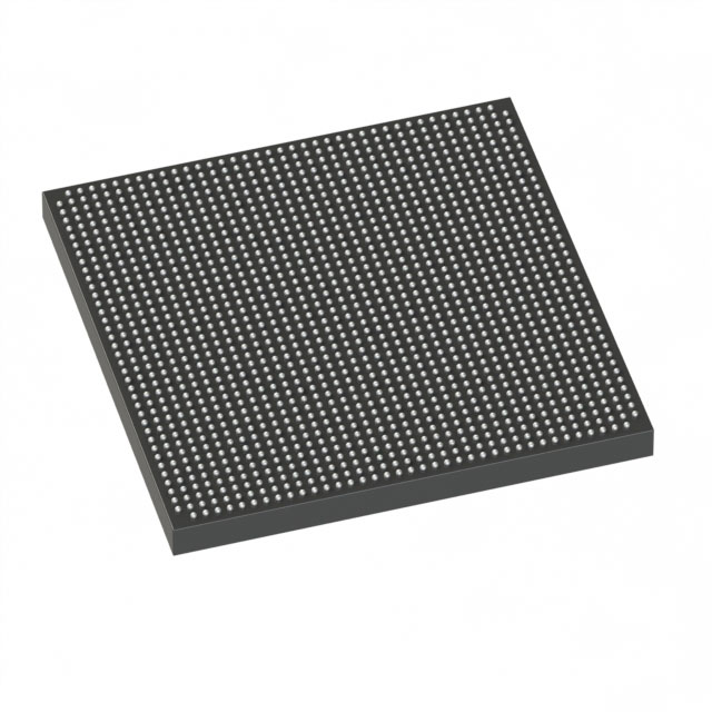
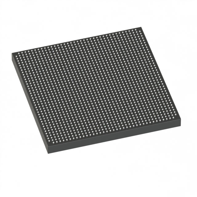
The 5SGXEABK2H40C2G is a Stratix® V GX family FPGA provided in a 1517-BBGA FCBGA package. It delivers very large on‑chip logic capacity and embedded memory, a high I/O count, and low-voltage core operation for commercial-grade system designs.
Engineered for applications that demand high logic density, substantial embedded RAM, and extensive connectivity, this device targets complex digital designs where integration and scalability are essential.
Key Features
- High logic capacity — 952,000 logic elements for implementing large-scale digital designs and complex custom logic.
- Logic array blocks (LABs) — 359,200 LABs to organize and structure large logic implementations.
- Embedded memory — Approximately 53.25 Mbits of on-chip RAM to support buffering, FIFOs, and on-device data storage.
- Extensive I/O — 696 I/O pins to support dense peripheral interfacing and multiple simultaneous high-pin-count connections.
- Package and mounting — 1517-BBGA (FCBGA) package; supplier device package listed as 1517-HBGA (45×45); surface-mount mounting type for PCB assembly.
- Low-voltage core — Core voltage supply range of 870 mV–930 mV for compatibility with low-voltage system architectures.
- Commercial temperature grade — Rated for operation from 0 °C to 85 °C for commercial electronic applications.
- Regulatory compliance — RoHS compliant.
Typical Applications
- High-density digital systems — Implement large custom logic blocks and complex state machines using the device’s 952,000 logic elements and 359,200 LABs.
- On-chip data buffering and memory‑intensive functions — Take advantage of approximately 53.25 Mbits of embedded RAM for packet buffering, FIFOs, and intermediate data storage without immediate need for external memory.
- High‑pin-count interfacing — Use the 696 I/O pins for multi‑lane interfaces, dense sensor arrays, or extensive control and monitoring signals.
Unique Advantages
- Massive programmable logic — 952,000 logic elements provide headroom for multi-domain designs and large-scale integration on a single device.
- Significant on‑chip memory — Approximately 53.25 Mbits of embedded RAM reduces reliance on external memory for many buffering and data‑path tasks.
- High I/O count — 696 I/Os enable complex connectivity and support for multiple high‑density interfaces simultaneously.
- Compact, surface‑mount package — 1517-BBGA (1517-HBGA supplier package, 45×45) balances pin density with a PCB‑friendly surface‑mount form factor.
- Low core voltage operation — 870 mV–930 mV core supply supports low‑voltage system designs and power-optimized architectures.
- Commercial-grade availability — Specified for 0 °C to 85 °C operation and RoHS compliance for commercial electronics manufacturing.
Why Choose 5SGXEABK2H40C2G?
The 5SGXEABK2H40C2G combines very large logic capacity, substantial embedded RAM, and a high I/O count in a single Stratix® V GX FPGA package. Its specifications make it suitable for demanding commercial designs that require dense programmable logic, significant on‑chip memory, and broad interfacing capability while operating within standard commercial temperature and low core-voltage ranges.
This device is well matched to engineering teams building complex digital systems that value integration and scalability. The combination of high logic element count, abundant embedded memory, and numerous I/Os supports consolidation of functions onto a single FPGA, contributing to more compact, maintainable system designs.
Request a quote or submit an inquiry to receive pricing, availability, or technical assistance for the 5SGXEABK2H40C2G.





















Date Founded: 1968
Headquarters: Santa Clara, California, USA
Employees: 130,000+
Revenue: $54.23 Billion
Certifications and Memberships: ISO9001:2015, ISO14001:2015, ISO17025:2017, ISO27001:2022, ISO45001:2018, ISO50001:2018


