
5SGXEB5R3F40C2LN
| Part Description |
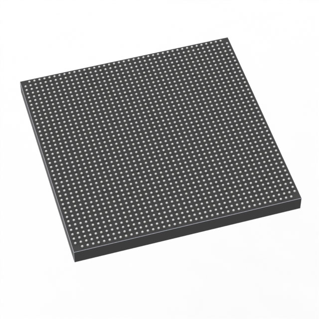
Stratix® V GX Field Programmable Gate Array (FPGA) IC 432 41984000 490000 1517-FBGA (40x40) |
|---|---|
| Quantity | 1,526 Available (as of June 14, 2026) |

| Product Category | Field Programmable Gate Array (FPGA) |
|---|---|
| Manufacturer | Intel |
| Manufacturing Status | Obsolete |
| Manufacturer Standard Lead Time | Contact Us |
| Datasheet |
Specifications & Environmental
| Device Package | 1517-FBGA (40x40) | Grade | Commercial | Operating Temperature | 0°C – 85°C | ||
|---|---|---|---|---|---|---|---|
| Package / Case | 1517-FBGA (40x40) | Number of I/O | 432 | Voltage | 820 mV - 880 mV | ||
| Mounting Method | Surface Mount | RoHS Compliance | RoHS Compliant | REACH Compliance | REACH Unknown | ||
| Moisture Sensitivity Level | 3 (168 Hours) | Number of LABs/CLBs | 185000 | Number of Logic Elements/Cells | 490000 | ||
| Number of Gates | N/A | ECCN | 3A001A2C | HTS Code | 8542.39.0001 | ||
| Qualification | N/A | Total RAM Bits | 41984000 |
Overview of 5SGXEB5R3F40C2LN – Stratix® V GX Field Programmable Gate Array (FPGA)
The 5SGXEB5R3F40C2LN is a Stratix V GX family FPGA offered in a 1517‑FBGA (40×40) package for surface‑mount assembly. It delivers high logic density with 490,000 logic elements and approximately 42 Mbits of embedded memory, along with 432 user I/Os, making it suitable for complex, programmable digital designs within commercial temperature environments.
Device operating parameters include a core voltage supply range of 820 mV to 880 mV and a commercial operating temperature range of 0 °C to 85 °C. The Stratix V series documentation also describes GX transceiver speed grade options within the family.
Key Features
- Logic Density 490,000 logic elements (cells) to implement large-scale, highly parallel hardware designs.
- Embedded Memory Approximately 42 Mbits of on‑chip RAM for buffering, lookup tables, and on‑chip data storage.
- I/O Count 432 user I/Os to support wide datapaths and complex peripheral interfacing.
- Package & Mounting 1517‑FBGA (40×40) supplier device package, supplied for surface mount PCB assembly.
- Power Supply Core voltage supply specified from 820 mV to 880 mV, enabling predictable power budgeting at the core rail.
- Temperature Grade Commercial grade operation with an ambient range of 0 °C to 85 °C.
- Regulatory Status RoHS compliant.
Typical Applications
- High‑density programmable logic Implement large, custom hardware accelerators and state machines that require hundreds of thousands of logic elements and sizable on‑chip RAM.
- Wide I/O systems Support designs needing extensive parallel interfaces or multiple high‑pin I/O peripherals using 432 available I/Os.
- Package‑constrained designs Deploy in compact 1517‑FBGA footprint applications where a surface‑mount, high‑pin‑count package is required.
Unique Advantages
- High logic capacity: 490,000 logic elements provide the headroom to integrate complex functions and consolidate multiple discrete devices into a single FPGA.
- Substantial on‑chip RAM: Approximately 42 Mbits of embedded memory reduces external memory dependency and simplifies board-level design.
- Extensive I/O: 432 user I/Os enable broad interfacing options for parallel data buses, board-level connectivity, or mixed-signal front ends.
- Commercial temperature support: Rated for 0 °C to 85 °C operation to meet standard commercial electronics deployment requirements.
- Compact package: 1517‑FBGA (40×40) provides a high‑pin‑count solution in a compact surface‑mount form factor.
- Standards‑aligned supply requirements: Defined core supply range (820 mV–880 mV) simplifies power rail design and system integration.
Why Choose 5SGXEB5R3F40C2LN?
The 5SGXEB5R3F40C2LN offers a balanced combination of high logic density, significant embedded memory, and extensive I/O in a compact FBGA package for commercial‑grade applications. Its clearly specified core voltage range and operating temperature band make it straightforward to integrate into power‑ and thermal‑managed systems.
This FPGA is well suited for designers who need to consolidate complex digital functions into a single programmable device while keeping board footprint and component count controlled. Its feature set aligns with projects that demand large programmable logic resources and on‑chip memory while operating in commercial environments.
If you would like pricing, lead‑time, or availability information for 5SGXEB5R3F40C2LN, request a quote or submit an inquiry and our team will respond with the details you need.


Date Founded: 1968
Headquarters: Santa Clara, California, USA
Employees: 130,000+
Revenue: $54.23 Billion
Certifications and Memberships: ISO9001:2015, ISO14001:2015, ISO17025:2017, ISO27001:2022, ISO45001:2018, ISO50001:2018


