
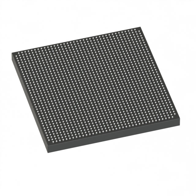
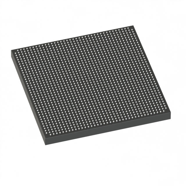
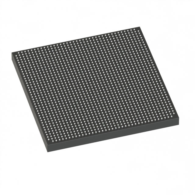
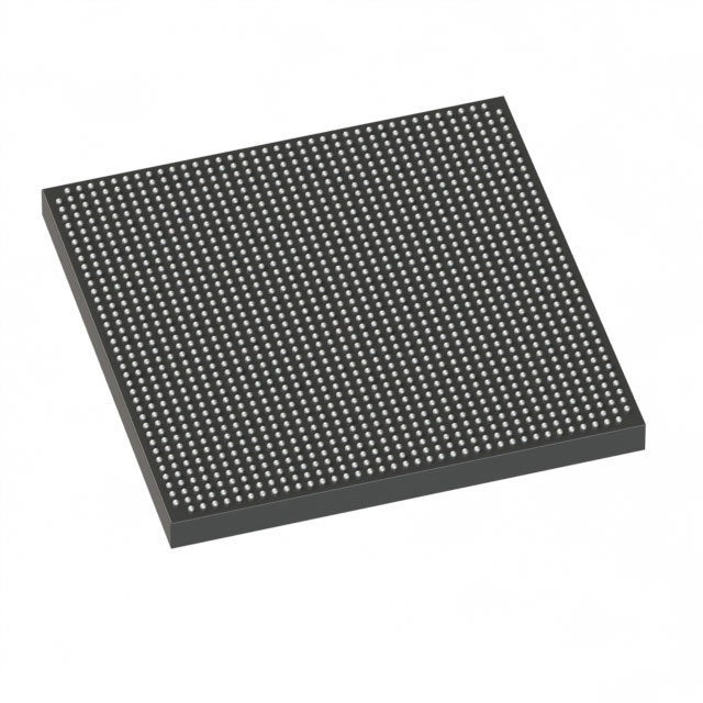
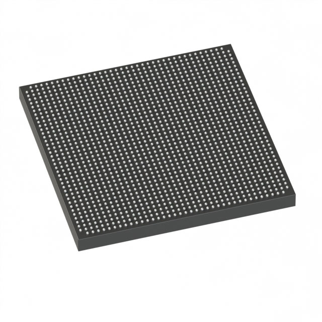
5SGXEB5R3F40I3LN
| Part Description |
Stratix® V GX Field Programmable Gate Array (FPGA) IC 432 41984000 490000 1517-FBGA (40x40) |
|---|---|
| Quantity | 1,354 Available (as of October 8, 2026) |
| Product Category | Field Programmable Gate Array (FPGA) |
|---|---|
| Manufacturer | Intel |
| Manufacturing Status | Obsolete |
| Manufacturer Standard Lead Time | Contact Us |
| Datasheet |
Specifications & Environmental
| Device Package | 1517-FBGA (40x40) | Grade | Industrial | Operating Temperature | -40°C – 100°C | ||
|---|---|---|---|---|---|---|---|
| Package / Case | 1517-FBGA (40x40) | Number of I/O | 432 | Voltage | 820 mV - 880 mV | ||
| Mounting Method | Surface Mount | RoHS Compliance | RoHS Compliant | REACH Compliance | REACH Unknown | ||
| Moisture Sensitivity Level | 3 (168 Hours) | Number of LABs/CLBs | 185000 | Number of Logic Elements/Cells | 490000 | ||
| Number of Gates | N/A | ECCN | 3A001A2C | HTS Code | 8542.39.0001 | ||
| Qualification | N/A | Total RAM Bits | 41984000 |
Overview of 5SGXEB5R3F40I3LN – Stratix® V GX Field Programmable Gate Array (FPGA) IC
The 5SGXEB5R3F40I3LN is a Stratix® V GX Field Programmable Gate Array (FPGA) IC from Intel, delivering very high logic density and substantial on-chip memory for complex digital systems. As a GX-class Stratix V device, it is documented within the Stratix V device family electrical and switching characteristics and is intended for industrial-grade applications that require large programmable logic resources, abundant I/O, and multi‑gigabit transceiver capability (transceiver performance is device and speed‑grade dependent).
Key Features
- Logic Capacity — 490,000 logic element cells for implementing large-scale custom logic and system functions.
- Embedded Memory — Approximately 42 Mbits of on‑chip RAM to support buffering, FIFOs, and memory‑intensive functions without external memory.
- I/O — 432 user I/O pins to interface with peripherals, sensors, and high-speed interfaces.
- Transceiver Capability — Stratix V GX devices include multi‑gigabit serial transceiver options (transceiver speed is dependent on device and speed grade as documented in the Stratix V datasheet).
- Power Supply — Core supply operating range from 820 mV to 880 mV to match system power architectures.
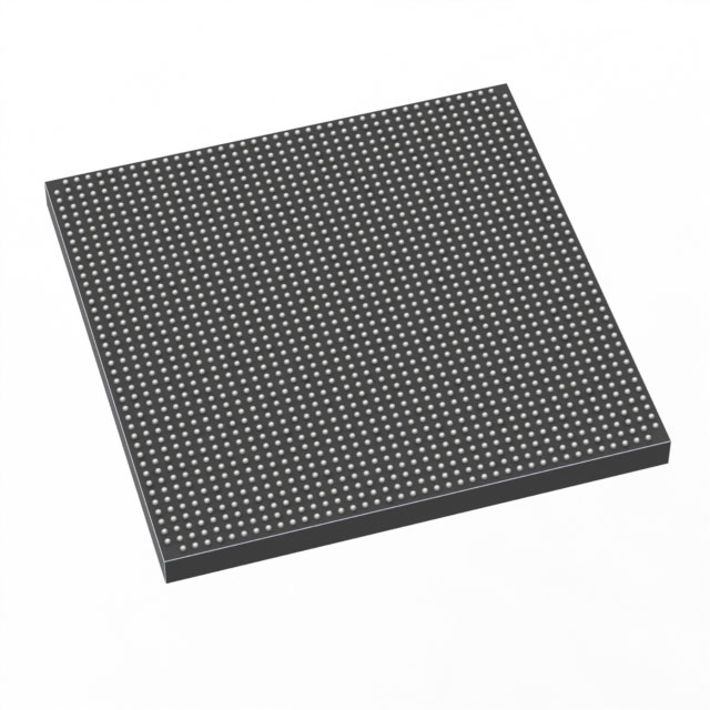
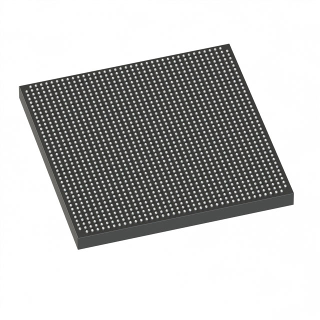
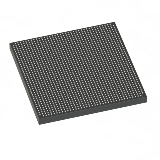
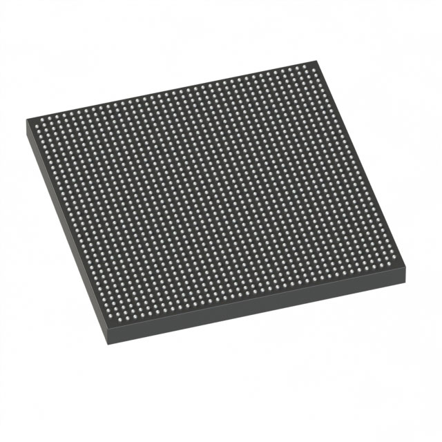
- Package & Mounting — Supplied in a 1517‑FBGA (40×40) package for surface-mount assembly.
- Industrial Temperature Grade — Rated for operation from −40 °C to 100 °C for deployment in demanding environments.
- Standards Compliance — RoHS compliant.
Typical Applications
- High‑performance networking — Implement packet processing, protocol offload, and multi‑gigabit serial interfaces using the device’s large logic and transceiver options.
- Signal processing and compute acceleration — Use abundant logic elements and on‑chip RAM for DSP pipelines, custom accelerators, and real‑time data processing.
- Industrial control and automation — Leverage extended temperature range and plentiful I/O for robust control, monitoring, and motor/servo interface functions.
- Storage and interconnect — Build host/controller logic and high‑speed interfaces that benefit from integrated memory and multi‑gigabit serial connectivity.
Unique Advantages
- High logic density: 490,000 logic element cells enable consolidation of multiple functions and system‑level integration into a single device.
- Significant embedded memory: Approximately 42 Mbits of RAM reduces reliance on external memory for buffering and state storage, simplifying board design.
- Large I/O complement: 432 I/O pins provide flexibility for diverse peripheral connectivity and high‑pin‑count interfaces.
- Industrial robustness: −40 °C to 100 °C operating range supports deployment in harsh or temperature‑variable environments.
- Compact BGA package: 1517‑FBGA (40×40) balances a high pin count with a compact footprint for space‑constrained systems.
- Documented electrical and switching characteristics: Device behavior, core and periphery performance, and I/O timing are covered in the Stratix V device datasheet for engineering reference.
Why Choose 5SGXEB5R3F40I3LN?
The 5SGXEB5R3F40I3LN positions itself as a high‑capacity, industrial‑grade FPGA option within the Stratix V GX family, combining nearly half a million logic element cells with roughly 42 Mbits of embedded RAM and a large I/O complement. Its operating voltage range and documented electrical and switching characteristics make it suitable for designs that demand substantial on‑chip resources, deterministic performance, and extended temperature operation.
This device is appropriate for engineering teams building complex networking, signal processing, industrial control, or storage/interface systems that benefit from consolidating logic, memory, and high‑speed serial capability into a single programmable device.
Request a quote or submit an inquiry to receive pricing and availability information for the 5SGXEB5R3F40I3LN FPGA.





















Date Founded: 1968
Headquarters: Santa Clara, California, USA
Employees: 130,000+
Revenue: $54.23 Billion
Certifications and Memberships: ISO9001:2015, ISO14001:2015, ISO17025:2017, ISO27001:2022, ISO45001:2018, ISO50001:2018


