
5SGXEB5R3F40I4G
| Part Description |
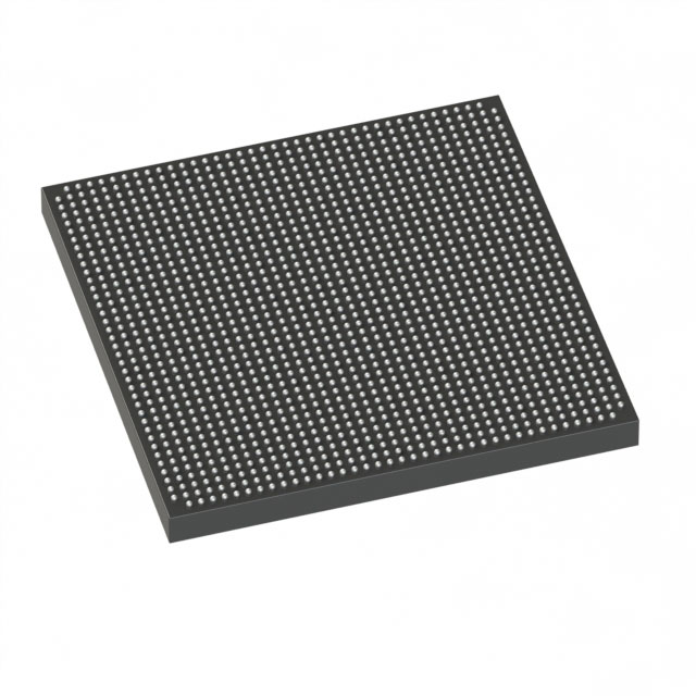
Stratix® V GX Field Programmable Gate Array (FPGA) IC 432 41984000 490000 1517-FBGA (40x40) |
|---|---|
| Quantity | 928 Available (as of June 15, 2026) |

| Product Category | Field Programmable Gate Array (FPGA) |
|---|---|
| Manufacturer | Intel |
| Manufacturing Status | Active |
| Manufacturer Standard Lead Time | 26 Weeks |
| Datasheet |
Specifications & Environmental
| Device Package | 1517-FBGA (40x40) | Grade | Industrial | Operating Temperature | -40°C – 100°C | ||
|---|---|---|---|---|---|---|---|
| Package / Case | 1517-FBGA (40x40) | Number of I/O | 432 | Voltage | 820 mV - 880 mV | ||
| Mounting Method | Surface Mount | RoHS Compliance | RoHS Compliant | REACH Compliance | REACH Unaffected | ||
| Moisture Sensitivity Level | 3 (168 Hours) | Number of LABs/CLBs | 185000 | Number of Logic Elements/Cells | 490000 | ||
| Number of Gates | N/A | ECCN | N/A | HTS Code | N/A | ||
| Qualification | N/A | Total RAM Bits | 41984000 |
Overview of 5SGXEB5R3F40I4G – Stratix® V GX FPGA, 490,000 logic elements, 1517‑FBGA (40×40)
The 5SGXEB5R3F40I4G is a Stratix® V GX field programmable gate array (FPGA) offered by Intel. It provides a high-density programmable fabric with 490,000 logic elements and approximately 42 Mbits of embedded memory, designed for demanding digital signal processing and high‑throughput designs.
Built for industrial environments, this device delivers a large I/O count and support for Stratix V GX transceiver speed grades documented in the device datasheet, making it suitable for high‑speed serial interfaces and complex system integration while operating across a wide temperature range.
Key Features
- Core density — 490,000 logic elements to implement large-scale digital designs and complex IP integrations.
- Programmable fabric resources — Approximately 42 Mbits of embedded RAM for on‑chip buffering, FIFOs, and memory‑intensive algorithms.
- I/O capacity — 432 user I/O pins to interface with high-pin-count systems and multiple peripherals.
- Transceiver capability (family) — Stratix V GX devices include transceiver speed grades documented in the Stratix V device datasheet, including 14.1 Gbps and 12.5 Gbps grades for appropriate GX configurations.
- Power supply — Core voltage range of 820 mV to 880 mV for the device core supply.
- Industrial temperature grade — Rated for operation from −40 °C to 100 °C for industrial deployments.
- Package and mounting — 1517‑FBGA (40×40) package in a surface‑mount form factor for board‑level integration.
- Regulatory compliance — RoHS compliant.
Typical Applications
- High‑performance signal processing — Use the large logic capacity and embedded RAM for real‑time DSP pipelines, FFTs, and algorithm acceleration.
- High‑speed serial systems — Leverage the Stratix V GX family transceiver grades for multi‑Gbps serial links and backplane communications.
- Industrial and embedded systems — Industrial temperature rating and robust I/O count make the device suitable for factory automation, industrial controllers, and measurement systems.
- Complex system integration — High logic density and abundant I/O support integration of multiple subsystems and custom accelerators on a single device.
Unique Advantages
- High integration density: 490,000 logic elements enable consolidation of large design functions into a single FPGA, reducing board complexity.
- Substantial on‑chip memory: Approximately 42 Mbits of embedded RAM supports large buffers and state storage without external memory.
- Extensive I/O: 432 I/O pins provide flexibility for interfacing with multiple peripherals, sensors, and high‑pin systems.
- Industrial‑grade operation: Rated for −40 °C to 100 °C, suitable for deployments requiring extended temperature range.
- Compact package: 1517‑FBGA (40×40) surface‑mount package balances high pin count with a manageable PCB footprint.
- Documented transceiver options: Stratix V GX devices include high‑speed transceiver speed grades as detailed in the device datasheet, supporting multi‑Gbps link requirements.
Why Choose 5SGXEB5R3F40I4G?
The 5SGXEB5R3F40I4G combines high logic capacity, significant on‑chip memory, and a large I/O complement in an industrial‑rated Stratix V GX FPGA package. It is aimed at engineers and system designers who require a programmable platform capable of implementing complex algorithms, high‑speed serial interfaces, and integrated system functions while operating across a wide temperature range.
With its dense fabric, documented transceiver speed grades, and compact 1517‑FBGA package, this device offers a scalable foundation for advanced embedded computing, communications, and industrial applications where integration and reliability are key.
Request a quote or submit a product inquiry to evaluate 5SGXEB5R3F40I4G for your next high‑density FPGA design.


Date Founded: 1968
Headquarters: Santa Clara, California, USA
Employees: 130,000+
Revenue: $54.23 Billion
Certifications and Memberships: ISO9001:2015, ISO14001:2015, ISO17025:2017, ISO27001:2022, ISO45001:2018, ISO50001:2018


