
5SGXEB6R1F40C2LN
| Part Description |
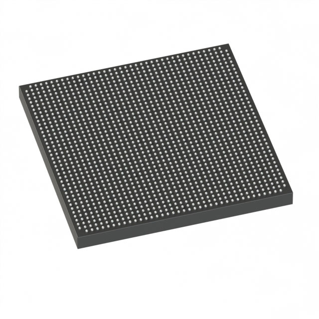
Stratix® V GX Field Programmable Gate Array (FPGA) IC 432 53248000 597000 1517-FBGA (40x40) |
|---|---|
| Quantity | 602 Available (as of June 15, 2026) |

| Product Category | Field Programmable Gate Array (FPGA) |
|---|---|
| Manufacturer | Intel |
| Manufacturing Status | Obsolete |
| Manufacturer Standard Lead Time | Contact Us |
| Datasheet |
Specifications & Environmental
| Device Package | 1517-FBGA (40x40) | Grade | Commercial | Operating Temperature | 0°C – 85°C | ||
|---|---|---|---|---|---|---|---|
| Package / Case | 1517-FBGA (40x40) | Number of I/O | 432 | Voltage | 820 mV - 880 mV | ||
| Mounting Method | Surface Mount | RoHS Compliance | RoHS Compliant | REACH Compliance | REACH Unknown | ||
| Moisture Sensitivity Level | 3 (168 Hours) | Number of LABs/CLBs | 225400 | Number of Logic Elements/Cells | 597000 | ||
| Number of Gates | N/A | ECCN | 3A001A2C | HTS Code | 8542.39.0001 | ||
| Qualification | N/A | Total RAM Bits | 53248000 |
Overview of 5SGXEB6R1F40C2LN – Stratix® V GX FPGA IC — 597,000 logic elements, approximately 53.25 Mbits RAM, 432 I/Os, 1517‑FBGA (40×40)
The 5SGXEB6R1F40C2LN is a Stratix V GX field‑programmable gate array (FPGA) from Intel, delivered in a 1517‑FBGA (40×40) surface‑mount package and specified for commercial temperature operation. The device combines a large programmable‑logic fabric with substantial on‑chip memory and extensive I/O to support complex digital designs.
Engineered for applications that require high logic capacity and dense I/O, this Stratix V GX device provides a balance of logic density, embedded memory, and transceiver‑oriented architecture as described in the Stratix V device documentation.
Key Features
- High Logic Capacity — 597,000 logic elements to accommodate large FPGA designs and complex datapath implementations.
- Embedded Memory — Approximately 53.25 Mbits of on‑chip RAM for buffering, on‑chip storage, and embedded data structures.
- Extensive I/O — 432 user I/Os to support wide external interfacing and dense board‑level connectivity.
- Package and Mounting — 1517‑FBGA (40×40) supplier device package supplied as a surface‑mount component for compact assembly.
- Core Voltage Range — Core voltage supply range of 820 mV to 880 mV, supporting designer control of core power rails.
- Commercial Grade Range — Specified operating temperature of 0 °C to 85 °C and listed as Commercial grade.
- Standards Compliance — RoHS‑compliant manufacturing status for environmental regulatory alignment.
Typical Applications
- High‑speed serial connectivity — Leverage the Stratix V GX transceiver‑oriented architecture (see device documentation) alongside the device’s large logic and memory resources to implement multi‑gigabit link logic and protocol processing.
- Network and communications processing — Use the abundant logic elements and on‑chip RAM for packet processing, buffering, and custom protocol acceleration.
- High‑density I/O systems — The 432 I/Os enable interfacing to a wide set of peripherals and parallel data busses for data‑capture and aggregation applications.
Unique Advantages
- Large programmable fabric: 597,000 logic elements provide headroom for complex algorithms, custom accelerators, and extensive control logic.
- Significant on‑chip memory: Approximately 53.25 Mbits of embedded RAM reduces dependence on external memory for many buffering and state‑storage needs.
- High I/O count: 432 I/Os simplify board routing for multi‑lane interfaces and parallel data paths, reducing external interface complexity.
- Compact, production‑ready package: The 1517‑FBGA (40×40) surface‑mount package balances pin density and board area for production designs.
- Controlled core power range: A defined 820 mV–880 mV supply window supports predictable core power provisioning and thermal planning.
- Regulatory alignment: RoHS compliance supports environmentally conscious manufacturing and procurement.
Why Choose 5SGXEB6R1F40C2LN?
The 5SGXEB6R1F40C2LN positions itself as a high‑capacity Stratix V GX FPGA option where large logic resources, substantial embedded RAM, and extensive I/O are required. Its commercial temperature rating and defined core voltage range make it suitable for production systems that demand predictable electrical and thermal characteristics.
Designers who need a dense programmable fabric with on‑chip memory and multi‑lane I/O capability will find this part aligned with medium‑to‑large FPGA designs. The device benefits from the Stratix V family documentation for electrical, switching and transceiver characteristics, supporting design validation and system integration.
If you would like pricing, availability, or a formal quote for 5SGXEB6R1F40C2LN, request a quote or submit an inquiry to receive details tailored to your project timeline and quantity requirements.


Date Founded: 1968
Headquarters: Santa Clara, California, USA
Employees: 130,000+
Revenue: $54.23 Billion
Certifications and Memberships: ISO9001:2015, ISO14001:2015, ISO17025:2017, ISO27001:2022, ISO45001:2018, ISO50001:2018


