
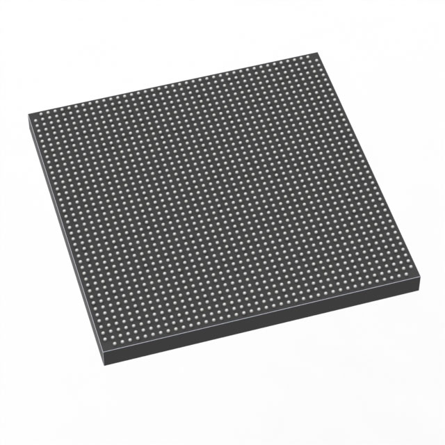
5SGXEB6R3F43I3G
| Part Description |
Stratix® V GX Field Programmable Gate Array (FPGA) IC 600 53248000 597000 1760-BBGA, FCBGA |
|---|---|
| Quantity | 1,182 Available (as of October 7, 2026) |
| Product Category | Field Programmable Gate Array (FPGA) |
|---|---|
| Manufacturer | Intel |
| Manufacturing Status | Active |
| Manufacturer Standard Lead Time | 26 Weeks |
| Datasheet |
Specifications & Environmental
| Device Package | 1760-FCBGA (42.5x42.5) | Grade | Industrial | Operating Temperature | -40°C – 100°C | ||
|---|---|---|---|---|---|---|---|
| Package / Case | 1760-BBGA, FCBGA | Number of I/O | 600 | Voltage | 820 mV - 880 mV | ||
| Mounting Method | Surface Mount | RoHS Compliance | RoHS Compliant | REACH Compliance | REACH Unaffected | ||
| Moisture Sensitivity Level | 3 (168 Hours) | Number of LABs/CLBs | 225400 | Number of Logic Elements/Cells | 597000 | ||
| Number of Gates | N/A | ECCN | N/A | HTS Code | N/A | ||
| Qualification | N/A | Total RAM Bits | 53248000 |
Overview of 5SGXEB6R3F43I3G – Stratix® V GX FPGA IC, 1760-FCBGA
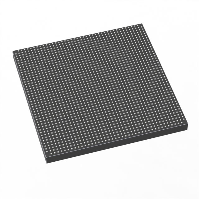
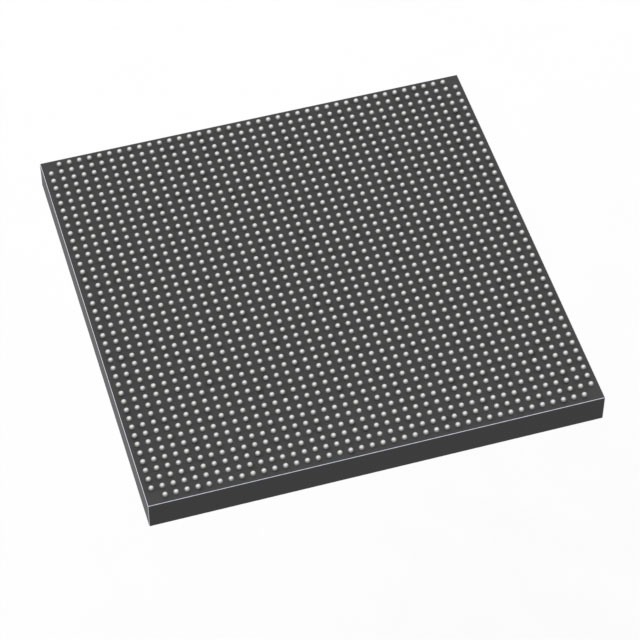
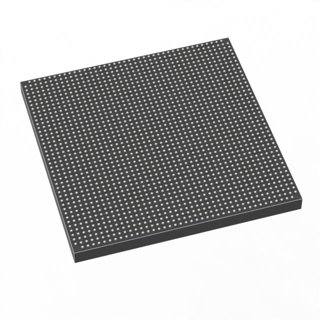
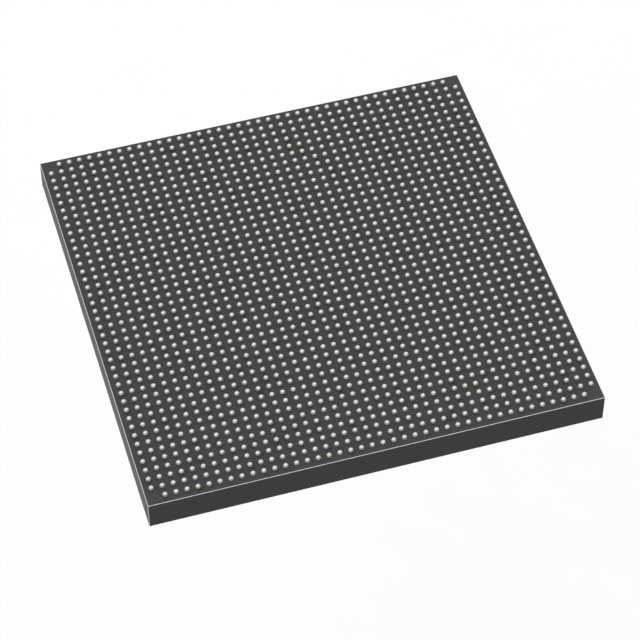
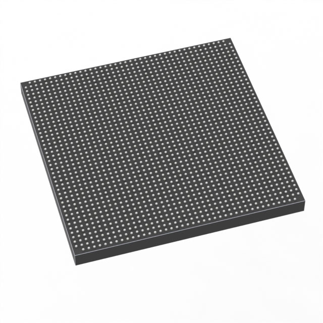
The 5SGXEB6R3F43I3G is an Intel Stratix® V GX field programmable gate array (FPGA) in a 1760-FCBGA package optimized for high-density logic, large on-chip memory, and extensive I/O. It is an industrial-grade device designed for applications that require significant programmable logic capacity and robust operating ranges.
This FPGA integrates approximately 597,000 logic elements, roughly 53.25 Mbits of embedded memory, and up to 600 I/O pins in a 1760-FCBGA (42.5 × 42.5 mm) package, with a core voltage supply in the 820 mV to 880 mV range and an operating temperature range of −40 °C to 100 °C.
Key Features
- Logic Capacity Approximately 597,000 logic elements for large-scale combinational and sequential logic integration.
- Embedded Memory Approximately 53.25 Mbits of on-chip RAM to support buffering, packet processing, and deep FIFOs without external memory.
- I/O Density Up to 600 I/O pins to accommodate high pin-count interfaces and complex board-level connectivity.
- Package & Mounting 1760-FCBGA package (42.5 × 42.5 mm), surface-mount mounting for compact, high-density board designs.
- Industrial Temperature Grade Rated for −40 °C to 100 °C operation for deployment in demanding industrial environments.
- Low-Voltage Core Core supply range of 820 mV to 880 mV supporting low-voltage operation consistent with modern FPGA architectures.
- Standards & Compliance RoHS compliant to meet environmental and regulatory requirements.
- Family Transceiver Capability (Series Data) Stratix V GX family device datasheet documents high-speed transceiver speed grades (example GX channel speeds include up to 14.1 Gbps in certain grades), as provided in the device series specification.
Typical Applications
- High‑performance Networking Use the device’s large logic and memory resources plus high I/O count for packet processing, line-rate switching, and protocol bridging.
- Data Center Acceleration Implement custom acceleration engines and data-path pipelines leveraging extensive on-chip RAM and logic capacity.
- Telecommunications Deploy as a programmable I/O and processing hub in systems that benefit from flexible serial/transceiver interfaces documented across the Stratix V GX family.
- Industrial Automation Take advantage of industrial temperature rating and high I/O density for machine control, data aggregation, and deterministic interfacing.
Unique Advantages
- High logic integration: Approximately 597,000 logic elements enable consolidation of multiple functions into a single device, reducing board-level complexity.
- Substantial on-chip memory: Approximately 53.25 Mbits of embedded RAM lowers dependence on external memory and improves data-path latency.
- Extensive I/O: Up to 600 I/Os support a wide range of parallel and serial interfaces without additional bridging components.
- Industrial robustness: Rated for −40 °C to 100 °C operation to suit harsh or temperature-variable deployments.
- Compact, high-density package: 1760-FCBGA (42.5 × 42.5 mm) provides a dense form factor for space-constrained, high-pin-count designs.
- Low-voltage core operation: 820 mV–880 mV supply range supports integration with modern low-voltage power architectures.
Why Choose 5SGXEB6R3F43I3G?
The 5SGXEB6R3F43I3G positions itself for designs that require large programmable logic resources, significant on-chip memory, and broad I/O capability within an industrial temperature envelope. Its combination of approximately 597,000 logic elements, approximately 53.25 Mbits of embedded RAM, and up to 600 I/Os in a 1760-FCBGA package provides a foundation for high-throughput, tightly integrated system designs.
This device is suitable for engineering teams building complex networking, data‑center acceleration, telecommunications, or industrial control applications where integration density, thermal range, and RoHS compliance are important selection criteria.
Request a quote or submit an inquiry to receive pricing, availability, and delivery information for the 5SGXEB6R3F43I3G Stratix V GX FPGA.





















Date Founded: 1968
Headquarters: Santa Clara, California, USA
Employees: 130,000+
Revenue: $54.23 Billion
Certifications and Memberships: ISO9001:2015, ISO14001:2015, ISO17025:2017, ISO27001:2022, ISO45001:2018, ISO50001:2018


