
5SGXEB6R3F43C4G
| Part Description |
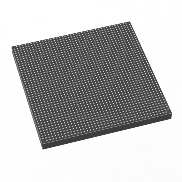
Stratix® V GX Field Programmable Gate Array (FPGA) IC 600 53248000 597000 1760-BBGA, FCBGA |
|---|---|
| Quantity | 42 Available (as of June 15, 2026) |

| Product Category | Field Programmable Gate Array (FPGA) |
|---|---|
| Manufacturer | Intel |
| Manufacturing Status | Active |
| Manufacturer Standard Lead Time | 26 Weeks |
| Datasheet |
Specifications & Environmental
| Device Package | 1760-FCBGA (42.5x42.5) | Grade | Commercial | Operating Temperature | 0°C – 85°C | ||
|---|---|---|---|---|---|---|---|
| Package / Case | 1760-BBGA, FCBGA | Number of I/O | 600 | Voltage | 820 mV - 880 mV | ||
| Mounting Method | Surface Mount | RoHS Compliance | RoHS Compliant | REACH Compliance | REACH Unaffected | ||
| Moisture Sensitivity Level | 3 (168 Hours) | Number of LABs/CLBs | 225400 | Number of Logic Elements/Cells | 597000 | ||
| Number of Gates | N/A | ECCN | N/A | HTS Code | N/A | ||
| Qualification | N/A | Total RAM Bits | 53248000 |
Overview of 5SGXEB6R3F43C4G – Stratix® V GX Field Programmable Gate Array (FPGA) IC
The 5SGXEB6R3F43C4G is a Stratix V GX family FPGA in a 1760‑FBGA package designed for commercial applications that require very high logic capacity, large embedded memory, and extensive I/O. As a Stratix V GX device, it is part of the Stratix V series documented in the Stratix V device datasheet and targets demanding digital designs where dense logic integration and rich I/O are key.
With 597,000 logic elements and approximately 53.248 Mbits of on‑chip RAM, this device supports complex, high‑capacity designs while offering a 600‑pin I/O interface and surface‑mount FCBGA packaging for board‑level integration.
Key Features
- Core Logic Approximately 597,000 logic elements to implement large, complex digital designs.
- Embedded Memory Approximately 53.248 Mbits of on‑chip RAM for deep buffering, look‑up tables, and state storage.
- I/O Density 600 I/O pins to support wide parallel interfaces, multiple peripherals, and complex board routing.
- Package & Mounting 1760‑FBGA (1760‑FCBGA) surface‑mount package; supplier package dimension listed as 1760‑FCBGA (42.5 × 42.5 mm) for system mechanical planning.
- Power Documented core supply range of 820 mV to 880 mV for core power planning and regulator selection.
- Temperature & Grade Commercial grade device with an operating temperature range of 0 °C to 85 °C.
- Standards & Compliance RoHS compliant.
- Stratix V GX Series Capabilities (datasheet) The Stratix V family datasheet documents GX transceiver speed grades; series examples include GX channel options such as 14.1 Gbps and 12.5 Gbps in defined speed grades.
Typical Applications
- High‑Performance Data Processing Large logic capacity and abundant on‑chip RAM enable complex packet processing, protocol handling, and custom compute pipelines.
- Networking & Telecom Large I/O count and Stratix V GX family transceiver capabilities (per datasheet) make this device suitable for board designs requiring extensive parallel and high‑speed interfaces.
- Prototyping & System Integration High logic density and rich I/O simplify integration of multi‑module systems and accelerate hardware development cycles.
Unique Advantages
- High Logic Density: 597,000 logic elements enable consolidation of large functions onto a single device, reducing board complexity.
- Significant Embedded Memory: Approximately 53.248 Mbits of on‑chip RAM supports buffering and on‑chip data structures without external memory in many use cases.
- Extensive I/O Connectivity: 600 I/Os accommodate broad peripheral sets and complex interfaces without multiplexing compromises.
- Board‑Level Packaging: 1760‑FBGA/FCBGA (42.5 × 42.5 mm) surface‑mount package supports high‑density PCB layouts and standard assembly processes.
- Defined Core Power Window: Core supply range of 820 mV–880 mV enables precise power delivery design and regulator selection for stable operation.
- Commercial Temperature Support: Rated for 0 °C to 85 °C operation for mainstream commercial deployments.
Why Choose 5SGXEB6R3F43C4G?
This Stratix V GX FPGA combines very high logic element capacity, substantial embedded memory, and a large I/O count in a single FCBGA package, making it a fit for commercial designs that demand consolidation of complex digital functions. Use this device when you need to implement extensive custom logic, on‑chip buffering, and broad peripheral connectivity within a surface‑mount board design.
Backed by the Stratix V family documentation and datasheet, the part provides a clear specification set for power, temperature, package, and series transceiver characteristics to support reliable system design and integration planning.
Request a quote or submit an inquiry to receive pricing, availability, and additional technical support for 5SGXEB6R3F43C4G.


Date Founded: 1968
Headquarters: Santa Clara, California, USA
Employees: 130,000+
Revenue: $54.23 Billion
Certifications and Memberships: ISO9001:2015, ISO14001:2015, ISO17025:2017, ISO27001:2022, ISO45001:2018, ISO50001:2018


