
5SGXMA3K2F35I3WN
| Part Description |
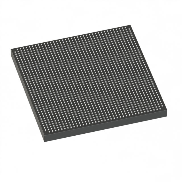
Stratix® V GX Field Programmable Gate Array (FPGA) IC 600 19456000 340000 1152-BBGA, FCBGA |
|---|---|
| Quantity | 1,237 Available (as of June 15, 2026) |

| Product Category | Field Programmable Gate Array (FPGA) |
|---|---|
| Manufacturer | Intel |
| Manufacturing Status | Obsolete |
| Manufacturer Standard Lead Time | Contact Us |
| Datasheet |
Specifications & Environmental
| Device Package | 1152-FBGA (35x35) | Grade | Industrial | Operating Temperature | -40°C – 100°C | ||
|---|---|---|---|---|---|---|---|
| Package / Case | 1152-BBGA, FCBGA | Number of I/O | 600 | Voltage | 820 mV - 880 mV | ||
| Mounting Method | Surface Mount | RoHS Compliance | RoHS non-compliant | REACH Compliance | REACH Unknown | ||
| Moisture Sensitivity Level | 4 (72 Hours) | Number of LABs/CLBs | 128300 | Number of Logic Elements/Cells | 340000 | ||
| Number of Gates | N/A | ECCN | OBSOLETE | HTS Code | N/A | ||
| Qualification | N/A | Total RAM Bits | 19456000 |
Overview of 5SGXMA3K2F35I3WN – Stratix® V GX Field Programmable Gate Array (FPGA)
The 5SGXMA3K2F35I3WN is a Stratix V GX family FPGA from Intel, delivered in a 1152-BBGA FCBGA package. It combines a high logic capacity and substantial on-chip memory with a large I/O complement for demanding industrial and high-performance embedded designs.
Designed for systems that require extensive programmable logic, on-chip RAM resources, and broad I/O connectivity, this device targets applications in communications, signal processing, and other compute-intensive markets where board-level integration and industrial temperature operation are required.
Key Features
- Core Logic Approximately 340,000 logic elements and 128,300 logic blocks provide the programmable capacity for complex RTL implementations and large custom datapaths.
- Embedded Memory Approximately 19.456 Mbits of on-chip RAM to support buffers, FIFOs, and on-chip storage for high-throughput designs.
- I/O Resources 600 user I/O pins to support wide parallel interfaces, large buses, and multi-channel connectivity.
- Package & Mounting 1152-BBGA (FCBGA) package; supplier device package listed as 1152-FBGA (35×35). Surface-mount package supports compact board-level integration.
- Power Supply Core supply operating range specified at 820 mV to 880 mV for the device core domain.
- Temperature Grade Industrial grade operation with an ambient operating range of −40 °C to 100 °C for deployment in industrial environments.
- Regulatory / Environmental RoHS compliant.
Typical Applications
- High-speed communications Large logic capacity and abundant I/O enable implementations of protocol offload, packet processing, and interface bridging for network equipment.
- Digital signal processing Substantial on-chip RAM and wide logic resources support real-time DSP chains, filtering, and custom accelerator functions.
- Data acquisition and instrumentation High I/O count and programmable logic density make the device suitable for multi-channel ADC/DAC front ends and custom measurement processing.
- Prototyping and emulation The device’s large logic and memory resources support complex SoC prototyping and hardware-software co-design environments.
Unique Advantages
- High programmable capacity: The combination of ~340,000 logic elements and 128,300 logic blocks enables large-scale logic integration without partitioning across multiple devices.
- Significant on-chip memory: Approximately 19.456 Mbits of embedded RAM reduces external memory dependence and improves throughput for streaming and buffering uses.
- Broad I/O connectivity: 600 I/O pins support complex interface mixes and high channel counts, simplifying system partitioning.
- Industrial temperature operation: Specified −40 °C to 100 °C operation suits deployments in industrial environments where extended temperature ranges are required.
- Compact FCBGA package: The 1152-ball FCBGA (35×35) package delivers high pin density in a compact footprint for space-constrained PCBs.
- RoHS compliant: Meets environmental compliance requirements for lead-free assembly and global manufacturing.
Why Choose 5SGXMA3K2F35I3WN?
The 5SGXMA3K2F35I3WN delivers a balance of high logic density, substantial embedded memory, and extensive I/O in an industrial-grade Stratix V GX device. It is positioned for engineers building high-throughput, compute- and I/O-intensive systems that require a compact, surface-mount FPGA solution backed by Intel’s Stratix V family documentation and support.
This device is suitable for designs that need scalability of logic and memory resources on a single device, enabling reduced BOM complexity and streamlined board layouts while maintaining operation across industrial temperature ranges.
Request a quote or submit an inquiry to start evaluating the 5SGXMA3K2F35I3WN for your next design. Technical documentation for the Stratix V family, including electrical and switching characteristics, is available from the manufacturer to support system integration and validation.


Date Founded: 1968
Headquarters: Santa Clara, California, USA
Employees: 130,000+
Revenue: $54.23 Billion
Certifications and Memberships: ISO9001:2015, ISO14001:2015, ISO17025:2017, ISO27001:2022, ISO45001:2018, ISO50001:2018


