
5SGXMA3K2F40C1WN
| Part Description |
Stratix® V GX Field Programmable Gate Array (FPGA) IC 600 19456000 340000 1517-BBGA, FCBGA |
|---|---|
| Quantity | 1,191 Available (as of June 15, 2026) |

| Product Category | Field Programmable Gate Array (FPGA) |
|---|---|
| Manufacturer | Intel |
| Manufacturing Status | Obsolete |
| Manufacturer Standard Lead Time | Contact Us |
| Datasheet |
Specifications & Environmental
| Device Package | 1517-FBGA (40x40) | Grade | Commercial | Operating Temperature | 0°C – 85°C | ||
|---|---|---|---|---|---|---|---|
| Package / Case | 1517-BBGA, FCBGA | Number of I/O | 600 | Voltage | 870 mV - 930 mV | ||
| Mounting Method | Surface Mount | RoHS Compliance | RoHS non-compliant | REACH Compliance | REACH Unknown | ||
| Moisture Sensitivity Level | 4 (72 Hours) | Number of LABs/CLBs | 128300 | Number of Logic Elements/Cells | 340000 | ||
| Number of Gates | N/A | ECCN | OBSOLETE | HTS Code | N/A | ||
| Qualification | N/A | Total RAM Bits | 19456000 |
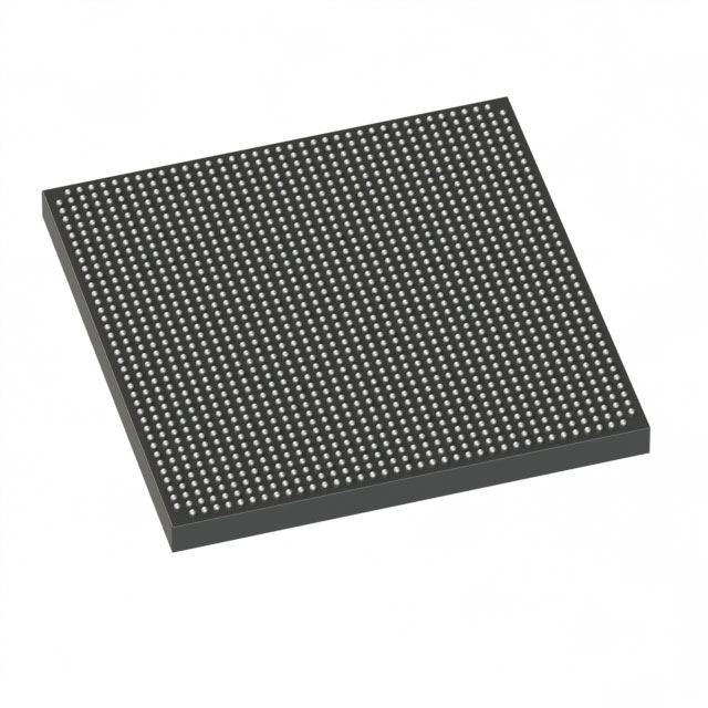
Overview of 5SGXMA3K2F40C1WN – Stratix® V GX FPGA, 340,000 logic elements, 600 I/O, 1517-BBGA
The 5SGXMA3K2F40C1WN is a Stratix® V GX Field Programmable Gate Array (FPGA) IC providing high-density programmable logic and extensive I/O in a 1517-BBGA (FCBGA) package. This commercial-grade device integrates 340,000 logic elements, approximately 19.456 Mbits of embedded memory, and 600 user I/O to support complex, logic- and memory-intensive designs.
Designed for surface-mount PCB assembly and operation in commercial environments, the device is specified for a core supply voltage range of 870 mV to 930 mV and an operating temperature range of 0 °C to 85 °C.
Key Features
- High Logic Density The device includes 340,000 logic elements suitable for complex digital designs and large-scale programmable implementations.
- Embedded Memory Approximately 19.456 Mbits of on-chip RAM supports data buffering, lookup tables, and memory-heavy algorithms without external memory for some workloads.
- Extensive I/O 600 available I/O pins provide broad interfacing capability for multi-channel systems and diverse peripheral connections.
- Package & Mounting 1517-BBGA (supplier package: 1517-FBGA, 40×40) package in a surface-mount format for compact, high-density board designs.
- Power Core supply voltage specified from 870 mV to 930 mV to match system power-rail planning and regulator selection.
- Commercial Temperature Grade Rated for operation from 0 °C to 85 °C for standard commercial applications.
- RoHS Compliant Device meets RoHS environmental requirements.
Typical Applications
- High-density digital processing Implementation of large-scale combinational and sequential logic where high logic element count and on-chip RAM are required.
- Prototype and system validation Hardware prototyping and SoC emulation that demand plentiful programmable logic and numerous I/O for external interfaces.
- I/O-intensive interfacing Designs needing many parallel or serial interfaces can leverage the device’s 600 I/O pins for connectivity and signal routing.
- Memory-centric acceleration On-chip embedded memory supports data buffering and lookup-based acceleration within the FPGA fabric.
Unique Advantages
- Large programmable fabric: 340,000 logic elements enable implementation of complex algorithms and large FPGA designs without immediate partitioning.
- Significant on-chip RAM: Approximately 19.456 Mbits of embedded memory reduces dependence on external memory for many data-intensive tasks.
- High I/O count: 600 I/O pins simplify integration with multi-peripheral systems and multi-channel interfaces, reducing external bridging logic.
- Compact BGA package: 1517-BBGA (40×40) package offers high pin density in a surface-mount form factor suitable for space-constrained boards.
- Commercial operating range: Specified 0 °C to 85 °C simplifies deployment in standard commercial applications and environments.
- Controlled core voltage: 870 mV–930 mV supply range supports predictable power budgeting and regulator selection.
Why Choose 5SGXMA3K2F40C1WN?
The 5SGXMA3K2F40C1WN positions itself as a high-density Stratix V GX FPGA for commercial designs that require substantial programmable logic, embedded memory, and a large I/O footprint in a compact BGA package. Its combination of 340,000 logic elements, approximately 19.456 Mbits of on-chip RAM, and 600 I/O pins addresses demanding digital processing, prototyping, and interface-rich applications.
This device is suited to teams and projects that need scalable FPGA capacity with clear electrical parameters—core supply between 870 mV and 930 mV—and commercial temperature operation. Its RoHS compliance and surface-mount 1517-BBGA package align with modern manufacturing and environmental requirements.
Request a quote or submit a product inquiry to obtain pricing, availability, and ordering information for 5SGXMA3K2F40C1WN.


Date Founded: 1968
Headquarters: Santa Clara, California, USA
Employees: 130,000+
Revenue: $54.23 Billion
Certifications and Memberships: ISO9001:2015, ISO14001:2015, ISO17025:2017, ISO27001:2022, ISO45001:2018, ISO50001:2018


