
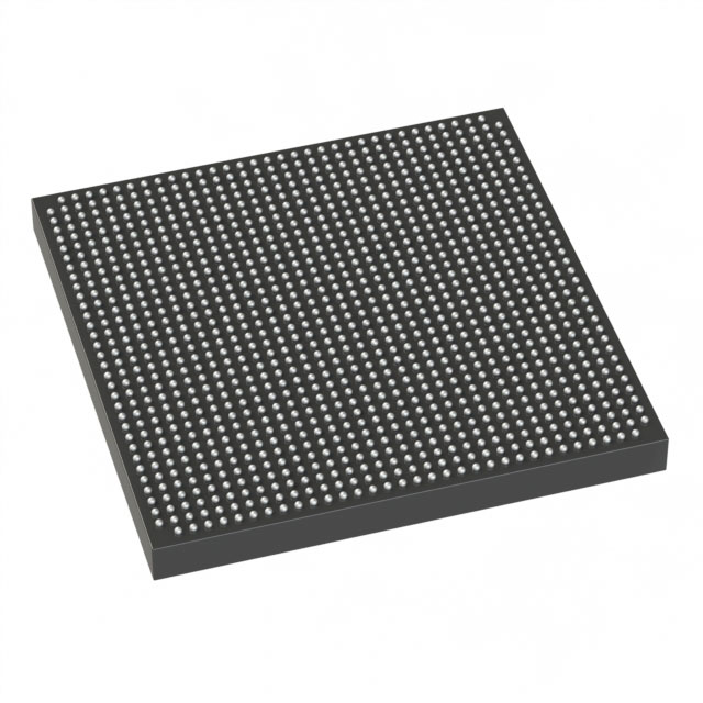
5SGXMA4H2F35C2
| Part Description |
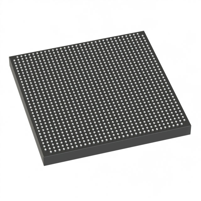
Stratix® V GX Field Programmable Gate Array (FPGA) IC 600 37888000 420000 1152-BBGA, FCBGA |
|---|---|
| Quantity | 307 Available (as of October 7, 2026) |
| Product Category | Field Programmable Gate Array (FPGA) |
|---|---|
| Manufacturer | Intel |
| Manufacturing Status | Obsolete |
| Manufacturer Standard Lead Time | Contact Us |
| Datasheet |
Specifications & Environmental
| Device Package | 1152-FBGA (35x35) | Grade | Commercial | Operating Temperature | 0°C – 85°C | ||
|---|---|---|---|---|---|---|---|
| Package / Case | 1152-BBGA, FCBGA | Number of I/O | 600 | Voltage | 870 mV - 930 mV | ||
| Mounting Method | Surface Mount | RoHS Compliance | RoHS non-compliant | REACH Compliance | REACH Unknown | ||
| Moisture Sensitivity Level | 3 (168 Hours) | Number of LABs/CLBs | 158500 | Number of Logic Elements/Cells | 420000 | ||
| Number of Gates | N/A | ECCN | 3A001A7A | HTS Code | 8542.39.0001 | ||
| Qualification | N/A | Total RAM Bits | 37888000 |
Overview of 5SGXMA4H2F35C2 – Stratix® V GX FPGA, 420,000 Logic Elements, 600 I/O, 1152-FBGA (35×35)
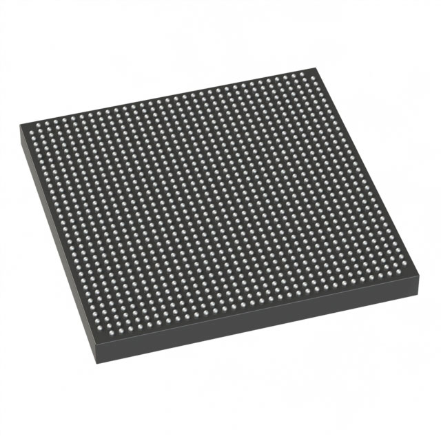
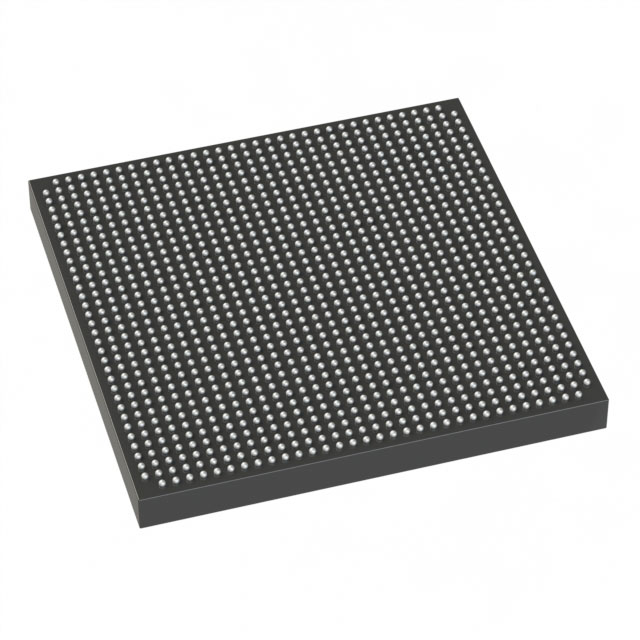
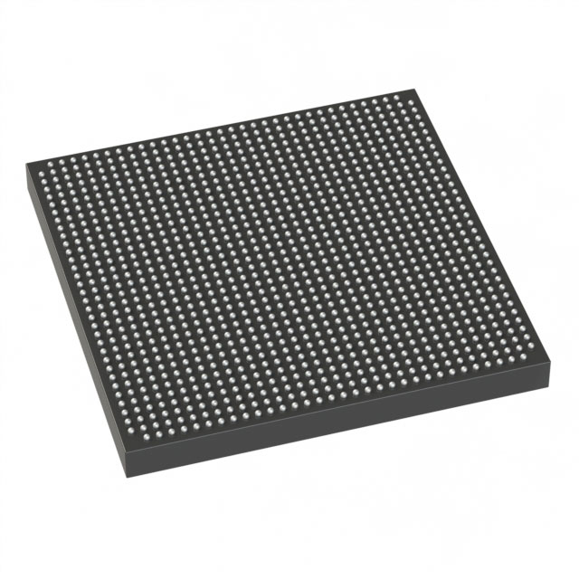
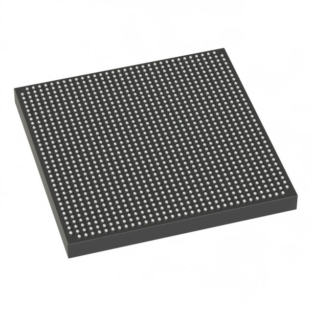
The 5SGXMA4H2F35C2 is a Stratix V GX field-programmable gate array (FPGA) in a 1152-ball FCBGA package, offering a high logic density fabric and a large I/O count for bandwidth-focused designs. Built on the Stratix V family architecture, this device combines a high count of logic elements, substantial on-chip memory, and the Stratix V GX series' transceiver capabilities to support data-intensive packet processing, optical transport, and high-performance DSP applications.
Key Features
- Logic Density — 420,000 logic elements to implement large, complex logic and control functions within a single device.
- Embedded Memory — Approximately 37.9 Mbits of on-chip RAM (37,888,000 bits) composed of M20K embedded memory blocks for buffering, packet storage, and fast local data access.
- I/O and Package — 600 I/O pins in a surface-mount 1152-FBGA (35×35) package, enabling high pin-count system interfaces and dense board routing.
- Transceiver Capability (Stratix V GX family) — Stratix V GX devices provide integrated serial transceivers (GX channels) targeted for high-bandwidth backplane and optical interfaces; the family supports multi-gigabit data rates suitable for 40G/100G transport and packet processing applications.
- Fabric and DSP — Stratix V family features a redesigned adaptive logic module (ALM), variable-precision DSP blocks, and a multi-track routing architecture to support high-performance signal processing workloads.
- Core and Power — 28-nm process technology with Stratix V family core voltage options (0.85 V or 0.9 V); this specific device lists a supply range of 870 mV to 930 mV.
- Clocking and Hard IP — Fractional PLLs, Embedded HardCopy Block for hardened IP instantiation (including PCIe Gen3/Gen2/Gen1), and fabric clocking resources to simplify system-level timing and IP integration.
- Operating Range and Compliance — Commercial grade device with an operating temperature range of 0 °C to 85 °C and RoHS compliance.
Typical Applications
- Optical transport and networking equipment — Use the high logic count, substantial embedded memory, and GX transceiver capabilities to implement 40G/100G line cards, multiplexing, and protocol handling.
- Packet processing and traffic management — Leverage abundant logic and I/O to implement deep packet inspection, forwarding engines, and high-throughput switching fabrics.
- High-performance DSP systems — Apply variable-precision DSP blocks and on-chip memory for signal processing pipelines in communications and test equipment.
- Test and measurement platforms — Combine large logic capacity and high I/O density to build flexible instrumentation and protocol analysis systems.
Unique Advantages
- High integration density: 420,000 logic elements reduce system BOM by consolidating complex logic into a single FPGA.
- Large on-chip memory: Approximately 37.9 Mbits of embedded RAM enables local buffering and high-performance data paths without external memory for many use cases.
- Extensive I/O capability: 600 I/Os in a 1152-FBGA package support diverse, high-pin-count interfaces and board-level routing flexibility.
- Transceiver-enabled bandwidth: As a Stratix V GX family device, it provides integrated serial transceivers suitable for high-bandwidth backplane and optical interfaces required by 40G/100G systems.
- IP and ASIC migration path: The Embedded HardCopy Block and Stratix V family roadmap support a low-risk transition path to hardened ASIC implementations where applicable.
- Commercial-grade reliability: Specified operating temperature (0 °C to 85 °C) and RoHS compliance for standard commercial applications.
Why Choose 5SGXMA4H2F35C2?
The 5SGXMA4H2F35C2 positions itself where high logic capacity, plentiful embedded memory, and broad I/O combine with family-level transceiver support to address bandwidth-centric and DSP-intensive designs. Its Stratix V architecture delivers the building blocks—ALMs, M20K memory, DSP blocks, fractional PLLs, and hard IP—that enable complex networking, transport, and processing applications.
This device is well suited for engineering teams developing high-throughput communications equipment, network test systems, and signal-processing platforms that require a scalable FPGA fabric with a practical path to hardened ASICs for production volume designs.
Request a quote or submit your design inquiry to receive pricing, availability, and technical support for 5SGXMA4H2F35C2.





















Date Founded: 1968
Headquarters: Santa Clara, California, USA
Employees: 130,000+
Revenue: $54.23 Billion
Certifications and Memberships: ISO9001:2015, ISO14001:2015, ISO17025:2017, ISO27001:2022, ISO45001:2018, ISO50001:2018


