
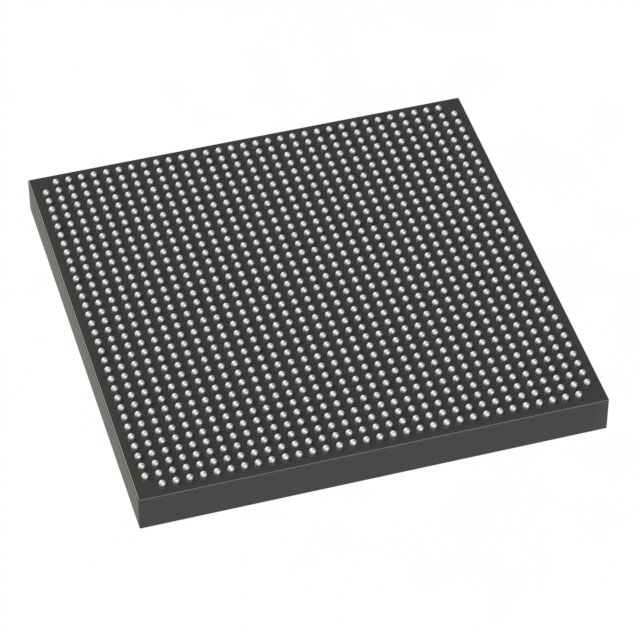
5SGXMA5H2F35C3N
| Part Description |
Stratix® V GX Field Programmable Gate Array (FPGA) IC 552 46080000 490000 1152-BBGA, FCBGA |
|---|---|
| Quantity | 971 Available (as of October 8, 2026) |
| Product Category | Field Programmable Gate Array (FPGA) |
|---|---|
| Manufacturer | Intel |
| Manufacturing Status | Obsolete |
| Manufacturer Standard Lead Time | Contact Us |
| Datasheet |
Specifications & Environmental
| Device Package | 1152-FBGA (35x35) | Grade | Commercial | Operating Temperature | 0°C – 85°C | ||
|---|---|---|---|---|---|---|---|
| Package / Case | 1152-BBGA, FCBGA | Number of I/O | 552 | Voltage | 820 mV - 880 mV | ||
| Mounting Method | Surface Mount | RoHS Compliance | RoHS Compliant | REACH Compliance | REACH Unknown | ||
| Moisture Sensitivity Level | 3 (168 Hours) | Number of LABs/CLBs | 185000 | Number of Logic Elements/Cells | 490000 | ||
| Number of Gates | N/A | ECCN | 3A001A2C | HTS Code | 8542.39.0001 | ||
| Qualification | N/A | Total RAM Bits | 46080000 |
Overview of 5SGXMA5H2F35C3N – Stratix® V GX FPGA — 490,000 logic elements, 552 I/Os, 1152-FBGA (35×35)
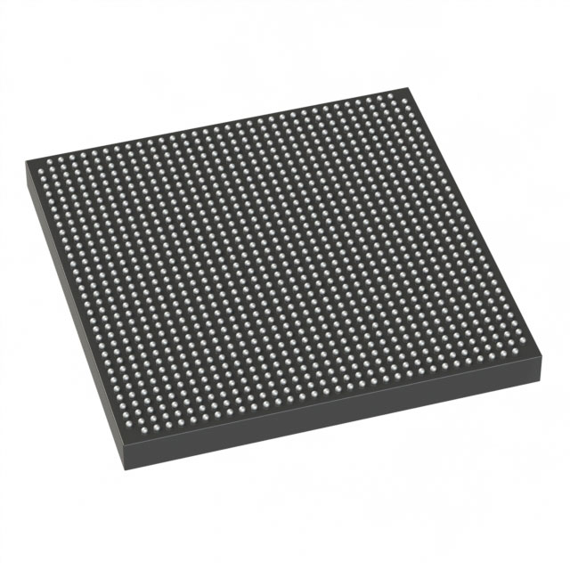
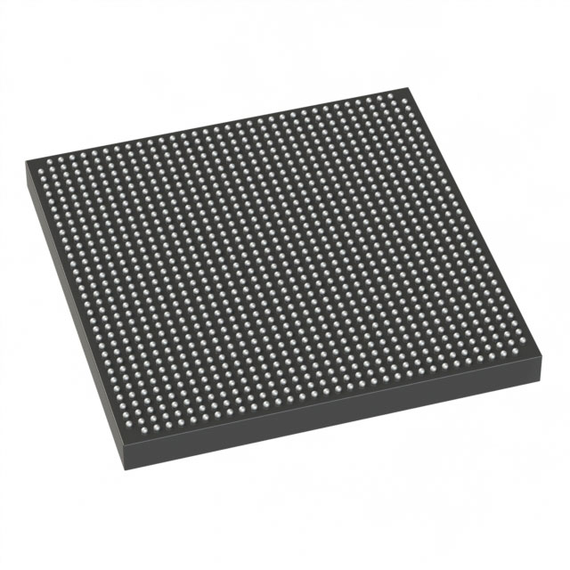
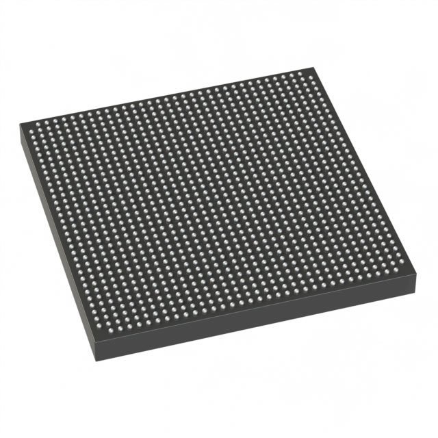
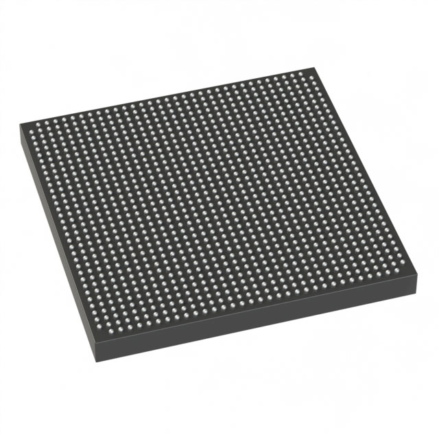
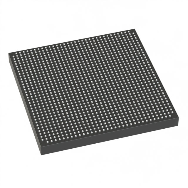
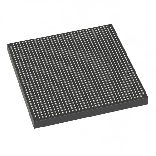
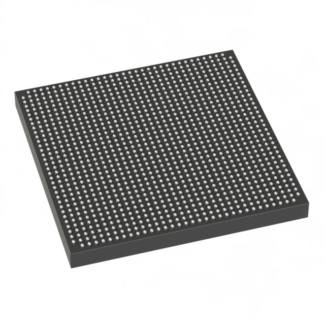
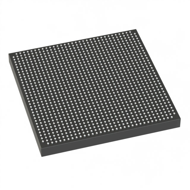
The 5SGXMA5H2F35C3N is a Stratix® V GX field programmable gate array (FPGA) in a 1152-pin FBGA package. It provides a large logic fabric, substantial on-chip memory, and a high I/O count for designs that require dense programmable logic and significant embedded RAM.
Designed for commercial-grade applications, the device operates from an 820 mV to 880 mV core supply and across a 0°C to 85°C temperature range, offering a balance of integration density and predictable operating conditions for complex digital systems.
Key Features
- Logic Capacity — 490,000 logic elements suitable for large-scale programmable designs and complex logic implementations.
- Embedded Memory — Approximately 46 Mbits of on-chip RAM to support data buffering, state retention, and memory-intensive logic blocks.
- I/O Density — 552 I/Os providing ample external connectivity for parallel interfaces, multi-channel I/O, and board-level integration.
- Transceiver Capabilities (Series) — Stratix V GX devices in the family support GX transceiver speed grades up to 14.1 Gbps, enabling high-speed serial connectivity where applicable.
- Power — Core voltage supply range of 820 mV to 880 mV for the device core.
- Package and Mounting — 1152-FBGA (35×35) package; surface-mount mounting type for standard PCB assembly.
- Commercial Temperature Grade — Rated for operation from 0°C to 85°C.
- RoHS Compliant — Meets RoHS environmental compliance requirements.
Typical Applications
- High-speed serial connectivity: Use family transceiver capability to implement multi-gigabit links and SerDes channels where high data-rate lanes are required.
- High-density logic systems: Leverage 490,000 logic elements and large embedded memory for complex control, data-path, and state-machine implementations.
- Multi-interface integration: 552 I/Os allow aggregation of parallel and serial interfaces, board-level bridging, and flexible peripheral connectivity.
- Prototyping and system integration: The device’s capacity and I/O count support integration of extensive IP blocks and system-level prototypes for verification and validation.
Unique Advantages
- High logic density: 490,000 logic elements reduce the need for multiple devices, simplifying board design and reducing BOM complexity.
- Substantial on-chip memory: Approximately 46 Mbits of embedded RAM enables local data buffering and accelerates memory-bound operations without external RAM.
- Extensive I/O resources: 552 I/Os provide flexibility for connecting multiple peripherals, parallel buses, and high-pin-count interfaces directly to the FPGA.
- Commercial temperature rating: Specified operation from 0°C to 85°C for deployment in standard commercial environments.
- RoHS compliance: Meets environmental requirements for regulated markets and designs.
- Standard surface-mount package: 1152-FBGA (35×35) supports industry-standard PCB assembly processes.
Why Choose 5SGXMA5H2F35C3N?
This Stratix V GX FPGA part combines a very large logic fabric with substantial embedded memory and a high I/O count, making it well suited for commercial designs that demand on-chip capacity and flexible connectivity. The device’s package density and surface-mount form factor simplify board-level integration while providing the headroom needed for complex system functions.
Choose 5SGXMA5H2F35C3N for projects that require scalable programmable logic, significant local memory, and wide I/O capability in a commercial-temperature FPGA offering with RoHS compliance.
Request a quote or submit an inquiry to check pricing, availability, and lead times for 5SGXMA5H2F35C3N. Our team can provide technical details and support to help evaluate this device for your design.





















Date Founded: 1968
Headquarters: Santa Clara, California, USA
Employees: 130,000+
Revenue: $54.23 Billion
Certifications and Memberships: ISO9001:2015, ISO14001:2015, ISO17025:2017, ISO27001:2022, ISO45001:2018, ISO50001:2018


