
5SGXMA5K1F40I2N
| Part Description |
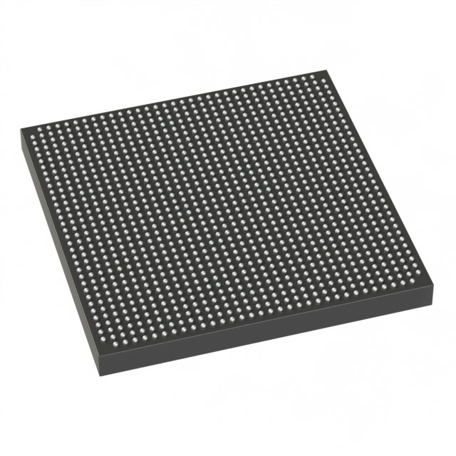
Stratix® V GX Field Programmable Gate Array (FPGA) IC 696 46080000 490000 1517-BBGA, FCBGA |
|---|---|
| Quantity | 981 Available (as of June 15, 2026) |

| Product Category | Field Programmable Gate Array (FPGA) |
|---|---|
| Manufacturer | Intel |
| Manufacturing Status | Obsolete |
| Manufacturer Standard Lead Time | Contact Us |
| Datasheet |
Specifications & Environmental
| Device Package | 1517-FBGA (40x40) | Grade | Industrial | Operating Temperature | -40°C – 100°C | ||
|---|---|---|---|---|---|---|---|
| Package / Case | 1517-BBGA, FCBGA | Number of I/O | 696 | Voltage | 870 mV - 930 mV | ||
| Mounting Method | Surface Mount | RoHS Compliance | RoHS Compliant | REACH Compliance | REACH Unknown | ||
| Moisture Sensitivity Level | 3 (168 Hours) | Number of LABs/CLBs | 185000 | Number of Logic Elements/Cells | 490000 | ||
| Number of Gates | N/A | ECCN | 3A001A2C | HTS Code | 8542.39.0001 | ||
| Qualification | N/A | Total RAM Bits | 46080000 |
Overview of 5SGXMA5K1F40I2N – Stratix® V GX Field Programmable Gate Array, 490,000 logic elements, 696 I/Os
The 5SGXMA5K1F40I2N is a Stratix V GX family Field Programmable Gate Array (FPGA) designed for high-density, programmable logic implementations in industrial environments. This device combines large logic capacity, substantial embedded memory, and a high I/O count to support complex, performance-oriented FPGA designs.
As a Stratix V GX device, the family documentation describes support for high-speed GX transceivers and a range of core and transceiver speed grades. The 5SGXMA5K1F40I2N is specified for industrial-grade deployment with a broad operating temperature range and RoHS compliance.
Key Features
- Logic Capacity — 490,000 logic elements (cells) to implement large, complex digital designs.
- Embedded Memory — Approximately 46 Mbits of on-chip RAM to support buffering, FIFOs, and on-chip data storage.
- I/O Resources — 696 user I/Os suitable for high pin-count interfaces and extensive peripheral connectivity.
- High-Speed Transceiver Family — Stratix V GX family documentation lists GX transceiver options; refer to the device datasheet for supported transceiver speed grades and channel capabilities.
- Power and Core Voltage — Core voltage supply range specified at 870 mV to 930 mV for the device core.
- Package & Mounting — 1517-BBGA FCBGA package (supplier device package: 1517-FBGA, 40×40) with surface-mount mounting type for board-level integration.
- Industrial Temperature Grade — Rated for operation from −40 °C to 100 °C for deployment in industrial environments.
- RoHS Compliant — Meets RoHS environmental requirements.
Typical Applications
- Communications Infrastructure — High logic density and Stratix V GX transceiver options suit protocol processing, switching, and high-throughput interfaces.
- Industrial Control & Automation — Industrial temperature rating and abundant I/O support robust control, motor drive, and data-acquisition implementations.
- High‑Density Signal Processing — Large logic element count and substantial on-chip RAM enable DSP pipelines, packet processing, and real-time data manipulation.
- FPGA Prototyping & System Development — Platform-scale resources and package options are applicable for complex system prototyping and hardware validation in development labs.
Unique Advantages
- High Logic Density: 490,000 logic elements provide the capacity to consolidate multiple functions into a single device, reducing board complexity.
- Substantial On‑Chip Memory: Approximately 46 Mbits of embedded RAM supports large buffering and on-chip data storage without external memory dependency.
- Extensive I/O Count: 696 I/Os enable broad peripheral connectivity and flexible interface routing for multi-protocol systems.
- Industrial Reliability: Rated for −40 °C to 100 °C operation, making the device suitable for industrial deployment conditions.
- Compact, Surface‑Mount Package: 1517-BBGA (FCBGA) 40×40 package balances high pin count with PCB area efficiency for dense system designs.
- Standards‑Aware Design Documentation: Stratix V device datasheet provides detailed electrical and switching characteristics to guide system-level integration and sizing.
Why Choose 5SGXMA5K1F40I2N?
The 5SGXMA5K1F40I2N positions itself for designs demanding high programmable logic capacity combined with significant on‑chip memory and a large number of I/Os. Its industrial temperature rating and RoHS compliance make it appropriate for long-lived, ruggedized applications where environmental margins matter.
Choose this FPGA when your project requires consolidating complex logic, extensive buffering, and flexible I/O in a single, surface-mount package while referencing the Stratix V family documentation for detailed transceiver and speed-grade planning.
Request a quote or submit an inquiry to obtain pricing, availability, and lead-time information for the 5SGXMA5K1F40I2N.


Date Founded: 1968
Headquarters: Santa Clara, California, USA
Employees: 130,000+
Revenue: $54.23 Billion
Certifications and Memberships: ISO9001:2015, ISO14001:2015, ISO17025:2017, ISO27001:2022, ISO45001:2018, ISO50001:2018


