
5SGXMA5K2F35C1N
| Part Description |
Stratix® V GX Field Programmable Gate Array (FPGA) IC 432 46080000 490000 1152-BBGA, FCBGA |
|---|---|
| Quantity | 799 Available (as of June 10, 2026) |
| Product Category | Field Programmable Gate Array (FPGA) |
|---|---|
| Manufacturer | Intel |
| Manufacturing Status | Obsolete |
| Manufacturer Standard Lead Time | Contact Us |
| Datasheet |
Specifications & Environmental
| Device Package | 1152-FBGA (35x35) | Grade | Commercial | Operating Temperature | 0°C – 85°C | ||
|---|---|---|---|---|---|---|---|
| Package / Case | 1152-BBGA, FCBGA | Number of I/O | 432 | Voltage | 870 mV - 930 mV | ||
| Mounting Method | Surface Mount | RoHS Compliance | RoHS Compliant | REACH Compliance | REACH Unknown | ||
| Moisture Sensitivity Level | 3 (168 Hours) | Number of LABs/CLBs | 185000 | Number of Logic Elements/Cells | 490000 | ||
| Number of Gates | N/A | ECCN | 3A001A2C | HTS Code | 8542.39.0001 | ||
| Qualification | N/A | Total RAM Bits | 46080000 |
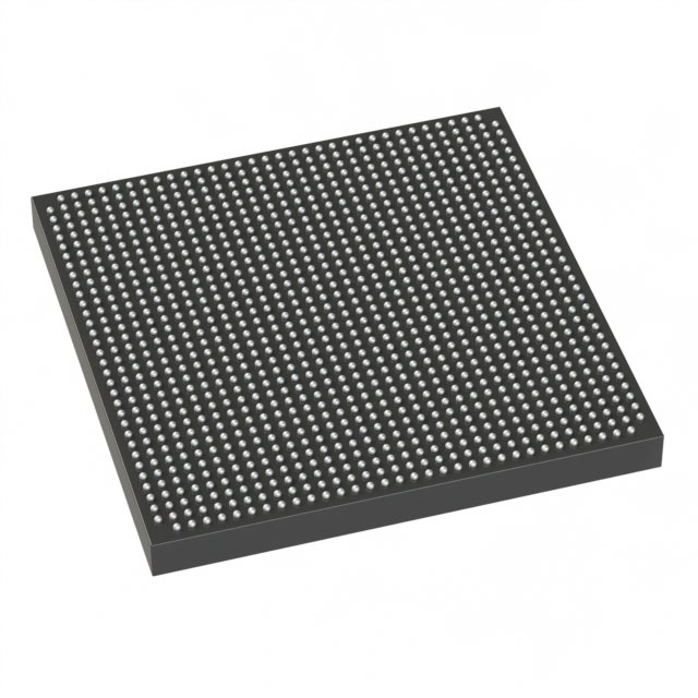
Overview of 5SGXMA5K2F35C1N – Stratix® V GX FPGA, 490,000 logic elements, 1152-FBGA
The 5SGXMA5K2F35C1N is a Stratix V GX field-programmable gate array offered in a 1152‑ball FCBGA package. It delivers high logic capacity and on-chip memory with a large I/O complement for demanding digital designs.
Targeted at commercial applications, this device combines 490,000 logic elements, approximately 46 Mbits of embedded RAM, and 432 I/O pins to support complex signal processing, high‑density logic integration, and multi‑interface designs while operating within a 0.87–0.93 V core supply range.
Key Features
- Core Capacity 490,000 logic elements (logic cells) for implementing large-scale custom logic and processing pipelines.
- Embedded Memory Approximately 46 Mbits of on-chip RAM to support buffering, packet storage, and stateful processing without immediate external memory dependence.
- I/O Density 432 I/O pins to enable broad peripheral and interface connectivity for multi‑lane and multi‑channel applications.
- Power and Supply Core voltage supply range of 0.87 V to 0.93 V for the device core, allowing predictable power domain planning.
- Package & Mounting 1152‑BBGA (FCBGA) package, supplier package listed as 1152‑FBGA (35×35); surface‑mount mounting type suited for modern PCB assembly.
- Temperature & Grade Commercial grade operation from 0 °C to 85 °C for standard commercial deployments.
- Compliance RoHS compliant, meeting common environmental restrictions for lead‑free manufacturing.
- Series-level Transceiver Information As documented for Stratix V GX devices in the series datasheet, GX transceiver speed grades are specified in the series documentation (series examples include GX channel speed options documented up to 14.1 Gbps).
Typical Applications
- High‑speed serial and networking interfaces High I/O count and Stratix V GX series transceiver capabilities (as documented in the series datasheet) support multi‑lane serial communications and interface aggregation.
- Signal processing and buffering Large on‑chip RAM and extensive logic resources enable real‑time data buffering, packet processing, and custom DSP pipelines.
- Complex control and protocol offload High logic density and plentiful I/O allow implementation of protocol stacks, offload engines, and custom control logic within a single device.
Unique Advantages
- High logic capacity: 490,000 logic elements provide substantial room for complex designs and feature-rich implementations without frequent FPGA family migration.
- Significant embedded memory: Approximately 46 Mbits of RAM reduces reliance on external memory for many buffering and state‑storage tasks, simplifying board design.
- Robust I/O complement: 432 I/O pins facilitate simultaneous connections to multiple peripherals, ADC/DAC front ends, or multi‑lane interfaces.
- Commercial temperature grade: Rated 0 °C to 85 °C for commercial deployments where standard operating conditions are expected.
- Standard surface‑mount package: 1152‑FBGA (35×35) package supports modern PCB assembly processes and high‑density board layouts.
- RoHS compliant: Conforms to common environmental manufacturing requirements for lead‑free production.
Why Choose 5SGXMA5K2F35C1N?
This Stratix V GX device balances high logic capacity, substantial on‑chip memory, and a large I/O count in a single commercial‑grade FCBGA package, making it suitable for complex digital designs that require integrated resources and flexible interfacing. It is a pragmatic choice for teams building high‑density logic, real‑time data processing, or multi‑interface systems who need predictable electrical and thermal operating parameters.
Backed by the Stratix V series documentation, the part provides a well‑documented foundation for transceiver and I/O timing considerations at the series level, enabling informed design tradeoffs and system integration planning.
Request a quote or submit a procurement inquiry for part number 5SGXMA5K2F35C1N to receive pricing and availability information. Include your quantity and target delivery timeline to expedite the response.


Date Founded: 1968
Headquarters: Santa Clara, California, USA
Employees: 130,000+
Revenue: $54.23 Billion
Certifications and Memberships: ISO9001:2015, ISO14001:2015, ISO17025:2017, ISO27001:2022, ISO45001:2018, ISO50001:2018


