
5SGXMA5K2F35C3N
| Part Description |
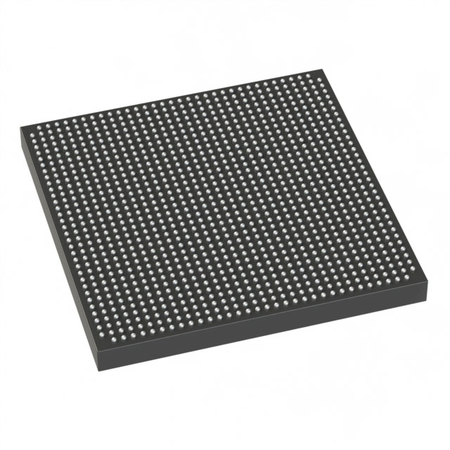
Stratix® V GX Field Programmable Gate Array (FPGA) IC 432 46080000 490000 1152-BBGA, FCBGA |
|---|---|
| Quantity | 684 Available (as of June 14, 2026) |

| Product Category | Field Programmable Gate Array (FPGA) |
|---|---|
| Manufacturer | Intel |
| Manufacturing Status | Obsolete |
| Manufacturer Standard Lead Time | Contact Us |
| Datasheet |
Specifications & Environmental
| Device Package | 1152-FBGA (35x35) | Grade | Commercial | Operating Temperature | 0°C – 85°C | ||
|---|---|---|---|---|---|---|---|
| Package / Case | 1152-BBGA, FCBGA | Number of I/O | 432 | Voltage | 820 mV - 880 mV | ||
| Mounting Method | Surface Mount | RoHS Compliance | RoHS Compliant | REACH Compliance | REACH Unknown | ||
| Moisture Sensitivity Level | 3 (168 Hours) | Number of LABs/CLBs | 185000 | Number of Logic Elements/Cells | 490000 | ||
| Number of Gates | N/A | ECCN | 3A001A2C | HTS Code | 8542.39.0001 | ||
| Qualification | N/A | Total RAM Bits | 46080000 |
Overview of 5SGXMA5K2F35C3N – Stratix® V GX Field Programmable Gate Array (FPGA) IC, 490,000 logic elements, 432 I/Os
The 5SGXMA5K2F35C3N is a Stratix V GX family FPGA manufactured by Intel. It provides a high-density programmable fabric with 490,000 logic elements and approximately 46 Mbits of embedded memory, targeted at commercial electronic systems that require significant on-chip logic and memory integration.
Designed for surface-mount board assembly in a 1152-BBGA (35×35) FCBGA package, the device delivers a large I/O count and low-voltage core operation (820 mV to 880 mV) within a commercial operating temperature range of 0 °C to 85 °C. Consult the Stratix V device datasheet for detailed electrical and switching characteristics, including I/O timing and transceiver information.
Key Features
- Programmable Logic Fabric — 490,000 logic elements to implement complex custom logic, state machines, and parallel processing functions.
- Embedded Memory — Approximately 46 Mbits of on-chip RAM for buffering, lookup tables, and memory-intensive algorithms.
- I/O Capacity — 432 user I/O pins to support dense board-level interfacing and multiple peripheral connections.
- Power and Core Voltage — Core supply voltage range of 820 mV to 880 mV to match system power design requirements.
- Package and Mounting — 1152-BBGA, FCBGA (supplier package 1152-FBGA, 35×35) optimized for high-density surface-mount PCB assembly.
- Commercial Temperature Grade — Rated for 0 °C to 85 °C operation for commercial applications.
- Standards Compliance — RoHS compliant for environmental and regulatory conformity.
Typical Applications
- High-density digital systems — Implement complex, large-scale logic with substantial on-chip memory to reduce external component count.
- Multi-channel I/O platforms — Leverage 432 I/Os to connect numerous peripherals, sensors, or high-pin-count interfaces on a single FPGA.
- Memory-intensive algorithms — Use approximately 46 Mbits of embedded RAM for buffering, packet processing, or intermediate data storage.
- Commercial electronic products — Deploy in products that operate within a 0 °C to 85 °C temperature range and require RoHS compliance.
Unique Advantages
- Large programmable fabric: 490,000 logic elements provide capacity for complex designs and high logic utilization.
- Substantial on-chip memory: Approximately 46 Mbits of embedded RAM reduces dependency on external memory components.
- High I/O density: 432 I/Os enable flexible interfacing and consolidation of multiple functions on a single device.
- Compact, manufacturing-friendly package: 1152-BBGA FCBGA (35×35) supports surface-mount assembly for compact, high-density PCBs.
- Low-voltage core operation: Core supply range of 820 mV–880 mV helps align with modern power-rail architectures.
- Commercial-grade suitability: Rated for 0 °C to 85 °C operation and RoHS compliant for many commercial product deployments.
Why Choose 5SGXMA5K2F35C3N?
The 5SGXMA5K2F35C3N delivers a balance of large-scale programmable logic, significant on-chip memory, and extensive I/O in a compact FCBGA package, making it well suited for commercial designs that require high integration and reduced external BOM. As a member of the Stratix V GX family from Intel, the device is documented in the Stratix V device datasheet, which provides detailed electrical, switching, and I/O timing characteristics to support system design and validation.
This FPGA is appropriate for designers and teams building complex, memory-rich programmable systems who need a commercially rated, RoHS-compliant device with a high I/O count and low-voltage core operation. Its feature set supports scalability across demanding digital and interface-intensive applications while aligning with standard commercial temperature and manufacturing requirements.
Request a quote or submit an RFQ to receive pricing and availability details for the 5SGXMA5K2F35C3N. Include part number and required quantity to expedite your inquiry.


Date Founded: 1968
Headquarters: Santa Clara, California, USA
Employees: 130,000+
Revenue: $54.23 Billion
Certifications and Memberships: ISO9001:2015, ISO14001:2015, ISO17025:2017, ISO27001:2022, ISO45001:2018, ISO50001:2018


