
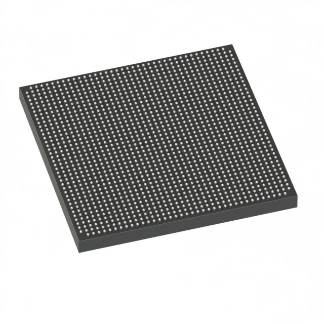
5SGXMA5K3F40C2N
| Part Description |
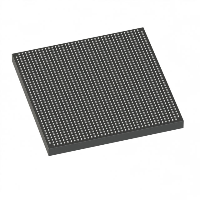
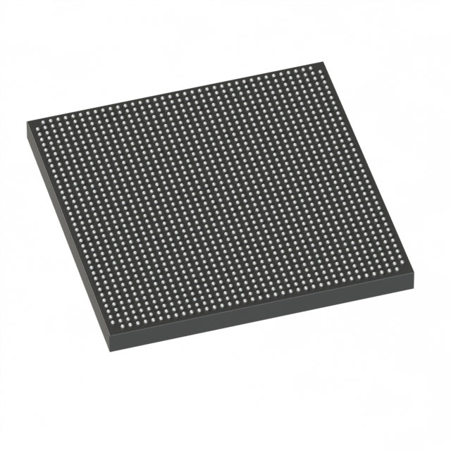
Stratix® V GX Field Programmable Gate Array (FPGA) IC 696 46080000 490000 1517-BBGA, FCBGA |
|---|---|
| Quantity | 1,566 Available (as of October 8, 2026) |
| Product Category | Field Programmable Gate Array (FPGA) |
|---|---|
| Manufacturer | Intel |
| Manufacturing Status | Obsolete |
| Manufacturer Standard Lead Time | Contact Us |
| Datasheet |
Specifications & Environmental
| Device Package | 1517-FBGA (40x40) | Grade | Commercial | Operating Temperature | 0°C – 85°C | ||
|---|---|---|---|---|---|---|---|
| Package / Case | 1517-BBGA, FCBGA | Number of I/O | 696 | Voltage | 870 mV - 930 mV | ||
| Mounting Method | Surface Mount | RoHS Compliance | RoHS Compliant | REACH Compliance | REACH Unknown | ||
| Moisture Sensitivity Level | 3 (168 Hours) | Number of LABs/CLBs | 185000 | Number of Logic Elements/Cells | 490000 | ||
| Number of Gates | N/A | ECCN | 3A001A2C | HTS Code | 8542.39.0001 | ||
| Qualification | N/A | Total RAM Bits | 46080000 |
Overview of 5SGXMA5K3F40C2N – Stratix® V GX FPGA, 490,000 Logic Elements, 1517-BBGA
The 5SGXMA5K3F40C2N is an Intel Stratix V GX Field Programmable Gate Array (FPGA) in a 1517-BBGA FCBGA package providing 490,000 logic elements and approximately 46 Mbits of embedded memory. Designed for high-density programmable logic implementations, this commercial‑grade device delivers a high I/O count and flexible power operation for demanding digital designs.
Key value drivers are large on‑chip memory, extensive I/O capability, and a compact surface‑mount FCBGA package that supports complex system integration where logic capacity and board‑level integration are priorities.
Key Features
- Logic Capacity 490,000 logic elements to implement large combinational and sequential logic networks.
- Embedded Memory Approximately 46 Mbits of on‑chip RAM for buffering, lookup tables, and embedded data storage.
- I/O Density 696 user I/Os to support wide parallel interfaces, multiple peripherals, and high‑pin‑count system connections.
- Package & Mounting 1517‑BBGA (FCBGA) package in a 1517‑FBGA (40×40) supplier footprint; surface‑mount mounting for compact board integration.
- Power Core supply range from 870 mV to 930 mV, enabling predictable power budgeting for core rails.
- Temperature & Grade Commercial grade with an operating temperature range of 0 °C to 85 °C.
- Regulatory Compliance RoHS‑compliant construction for environmental compliance in standard commercial applications.
Typical Applications
- High‑Density Digital Systems Implement large custom logic blocks and complex processing pipelines that require significant LUT and register resources.
- Data Buffering and Memory‑Intensive Functions Use on‑chip RAM for packet buffering, FIFOs, and lookup tables where fast local memory improves throughput.
- Interface‑Rich Platforms Leverage the high I/O count to connect multiple parallel buses, sensors, and peripheral interfaces on a single device.
- Prototyping and System Integration Deploy as a scalable platform for validating complex system architectures and consolidating multi‑chip logic into one FPGA.
Unique Advantages
- High Logic Density: 490,000 logic elements enable implementation of large-scale designs without extensive partitioning across multiple devices.
- Substantial On‑Chip Memory: Approximately 46 Mbits of embedded RAM reduces external memory dependence and improves latency for data‑critical paths.
- Extensive I/O Resources: 696 I/Os provide flexibility to support multiple parallel interfaces, complex board topologies, and large connector footprints.
- Compact FCBGA Package: 1517‑BBGA packaging offers a high‑pin‑count solution with a compact PCB footprint for space‑constrained designs.
- Predictable Power Envelope: Documented core voltage range (870–930 mV) allows accurate power budgeting during system design.
- RoHS Compliance: Designed for compliance with RoHS requirements for environmentally responsible manufacturing.
Why Choose 5SGXMA5K3F40C2N?
The 5SGXMA5K3F40C2N combines high logic capacity, meaningful on‑chip memory, and a large I/O complement in a compact surface‑mount FCBGA package—an attractive combination for engineers consolidating complex digital functions onto a single FPGA. Its commercial temperature grade and defined core voltage range make it suitable for production systems that require predictable operating conditions.
As a member of the Stratix V GX family, this device is positioned for designs that demand substantial programmable logic and integration density while retaining the advantages of an established FPGA series and available technical documentation.
Request a quote or submit an inquiry to receive pricing, availability, and lead time information for the 5SGXMA5K3F40C2N. Our team can assist with part selection and procurement details to support your project schedule.





















Date Founded: 1968
Headquarters: Santa Clara, California, USA
Employees: 130,000+
Revenue: $54.23 Billion
Certifications and Memberships: ISO9001:2015, ISO14001:2015, ISO17025:2017, ISO27001:2022, ISO45001:2018, ISO50001:2018


