
5SGXMA5K3F35I4WN
| Part Description |
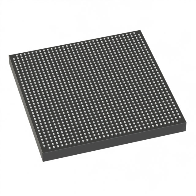
Stratix® V GX Field Programmable Gate Array (FPGA) IC 432 46080000 490000 1152-BBGA, FCBGA |
|---|---|
| Quantity | 1,608 Available (as of June 15, 2026) |

| Product Category | Field Programmable Gate Array (FPGA) |
|---|---|
| Manufacturer | Intel |
| Manufacturing Status | Obsolete |
| Manufacturer Standard Lead Time | Contact Us |
| Datasheet |
Specifications & Environmental
| Device Package | 1152-FBGA (35x35) | Grade | Industrial | Operating Temperature | -40°C – 100°C | ||
|---|---|---|---|---|---|---|---|
| Package / Case | 1152-BBGA, FCBGA | Number of I/O | 432 | Voltage | 820 mV - 880 mV | ||
| Mounting Method | Surface Mount | RoHS Compliance | RoHS non-compliant | REACH Compliance | REACH Unknown | ||
| Moisture Sensitivity Level | 4 (72 Hours) | Number of LABs/CLBs | 185000 | Number of Logic Elements/Cells | 490000 | ||
| Number of Gates | N/A | ECCN | OBSOLETE | HTS Code | N/A | ||
| Qualification | N/A | Total RAM Bits | 46080000 |
Overview of 5SGXMA5K3F35I4WN – Stratix® V GX FPGA, 1152-BBGA (35×35), Industrial
The 5SGXMA5K3F35I4WN is a Stratix® V GX Field Programmable Gate Array (FPGA) IC from Intel, supplied in a 1152-BBGA FCBGA package (35×35). It provides high logic density, abundant embedded RAM, and a large I/O count for designs that require substantial on-chip resources and flexible interfacing.
With industrial temperature grading and a defined core voltage range, this device is suited to applications that demand robust operation across extended temperature ranges and precise power delivery.
Key Features
- Logic Capacity Approximately 490,000 logic elements to implement large-scale, complex digital designs.
- Embedded Memory Approximately 46.08 Mbits of on-chip RAM for frame buffering, packet storage, and streaming data operations.
- I/O Resources 432 user I/Os to support wide parallel interfaces and multiple peripheral connections.
- Package & Mounting 1152-BBGA, FCBGA supply package (listed as 1152-FBGA 35×35); surface-mount device for high-density PCB integration.
- Power Supply Core voltage supply range: 820 mV to 880 mV, enabling precise core power budgeting in system design.
- Temperature & Grade Industrial grade with operating temperature range of –40 °C to 100 °C for applications requiring extended thermal tolerance.
- Standards Compliance RoHS compliant.
- Stratix V Family Documentation Part of the Stratix V GX device family; series documentation describes device electrical characteristics, operating conditions, and transceiver options for system-level planning.
Typical Applications
- High‑density digital processing Use the large logic and memory resources to implement complex signal processing, packet processing, or compute-acceleration functions.
- High‑pin-count systems Large I/O complement supports boards requiring extensive parallel interfaces, bus bridging, or multi‑port connectivity.
- Transceiver‑enabled designs As a Stratix V GX device, it aligns with system designs that exploit the family’s transceiver capabilities for high-rate serial links and protocol bridging (refer to family documentation for transceiver grade details).
Unique Advantages
- High on‑chip resource density: The combination of ~490,000 logic elements and ~46.08 Mbits of embedded RAM reduces the need for external memory and offloads system-level buffering.
- Ample I/O for system integration: 432 I/Os allow direct interfacing to a wide range of peripherals and parallel buses, simplifying board-level connectivity.
- Industrial temperature range: Rated from –40 °C to 100 °C for reliable operation in harsh or temperature-variable environments.
- Compact, surface-mount BBGA package: 1152-ball FCBGA (35×35) enables high-density PCB layouts while maintaining a standardized package footprint.
- Predictable core power requirement: Defined core supply range (820 mV–880 mV) supports precise power-supply design and thermal planning.
- RoHS compliant: Meets environmental compliance requirements for lead‑free assembly processes.
Why Choose 5SGXMA5K3F35I4WN?
This Stratix V GX device delivers a balance of large logic capacity, significant embedded memory, and extensive I/O in a single industrial‑grade FCBGA package. It is well suited to designs that demand on‑chip resources and robust thermal performance while maintaining a compact board footprint.
Engineers designing high-density digital systems, multi‑interface boards, or transceiver-enabled links can leverage the documented Stratix V family characteristics alongside this part’s specific resource set to scale and validate system architectures with confidence.
Request a quote or submit an RFQ to begin procurement of the 5SGXMA5K3F35I4WN for your next design.


Date Founded: 1968
Headquarters: Santa Clara, California, USA
Employees: 130,000+
Revenue: $54.23 Billion
Certifications and Memberships: ISO9001:2015, ISO14001:2015, ISO17025:2017, ISO27001:2022, ISO45001:2018, ISO50001:2018


