
5SGXMA5K3F40I3LG
| Part Description |
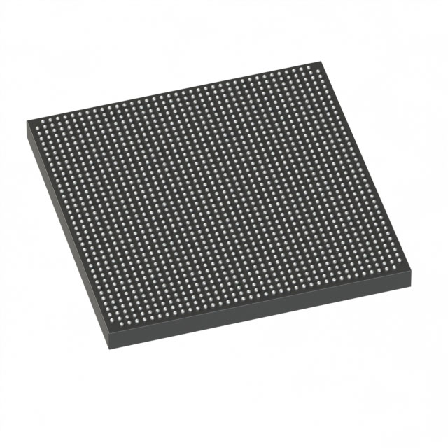
Stratix® V GX Field Programmable Gate Array (FPGA) IC 696 46080000 490000 1517-BBGA, FCBGA |
|---|---|
| Quantity | 1,366 Available (as of June 15, 2026) |

| Product Category | Field Programmable Gate Array (FPGA) |
|---|---|
| Manufacturer | Intel |
| Manufacturing Status | Active |
| Manufacturer Standard Lead Time | 26 Weeks |
| Datasheet |
Specifications & Environmental
| Device Package | 1517-FBGA (40x40) | Grade | Industrial | Operating Temperature | -40°C – 100°C | ||
|---|---|---|---|---|---|---|---|
| Package / Case | 1517-BBGA, FCBGA | Number of I/O | 696 | Voltage | 820 mV - 880 mV | ||
| Mounting Method | Surface Mount | RoHS Compliance | RoHS Compliant | REACH Compliance | REACH Unaffected | ||
| Moisture Sensitivity Level | 3 (168 Hours) | Number of LABs/CLBs | 185000 | Number of Logic Elements/Cells | 490000 | ||
| Number of Gates | N/A | ECCN | N/A | HTS Code | N/A | ||
| Qualification | N/A | Total RAM Bits | 46080000 |
Overview of 5SGXMA5K3F40I3LG – Stratix® V GX FPGA, 1517-FBGA (40×40), Industrial
The 5SGXMA5K3F40I3LG is a Stratix® V GX Field Programmable Gate Array (FPGA) from Intel, provided in a 1517-ball FCBGA package. It delivers high logic density, substantial embedded RAM, and extensive I/O for complex, programmable digital designs.
Designed for applications that require large on-chip resources and robust thermal range, this industrial-grade device combines approximately 490,000 logic elements, ~46.08 Mbits of embedded memory, and 696 user I/O in a surface-mount BGA package.
Key Features
- Core Logic — Approximately 490,000 logic elements to implement large-scale programmable logic and custom hardware acceleration.
- Embedded Memory — Approximately 46.08 Mbits of on-chip RAM to support buffering, FIFOs, and large local data structures without external memory.
- I/O Capacity — 696 user I/O pins for broad interfacing to peripherals, serializers, and parallel buses.
- Package & Mounting — 1517-BBGA (1517-FBGA, 40×40) surface-mount package optimized for high-density PCB layouts.
- Power — Core voltage supply range specified at 0.820 V to 0.880 V for the device core domain.
- Industrial Temperature Grade — Rated for operation from −40 °C to 100 °C for demanding ambient conditions.
- Compliance — RoHS compliant.
Typical Applications
- High-density signal processing — Use the large logic capacity and embedded memory for real-time packet processing, filtering, and algorithm acceleration.
- Multi-channel I/O aggregation — 696 I/O pins enable consolidation of many parallel and serial interfaces on a single device.
- Industrial systems — Industrial temperature rating and robust package make it suitable for factory automation, test equipment, and instrumentation.
- Transceiver-enabled designs — As a GX device in the Stratix V family, it supports designs that incorporate high-performance serial/transceiver subsystems.
Unique Advantages
- High logic capacity: Approximately 490,000 logic elements reduce the need for multi-device partitioning and simplify system architecture.
- Large on-chip RAM: ~46.08 Mbits of embedded memory supports deep buffering and complex state machines without external memory overhead.
- Extensive I/O integration: 696 I/O pins provide flexibility for mixed-signal front ends, large bus interfaces, and dense connector layouts.
- Industrial operating range: −40 °C to 100 °C supports deployment in harsher environments and extended-temperature applications.
- Compact BGA package: 1517-FBGA (40×40) delivers high pin count in a space-efficient footprint for PCB real estate savings.
- Low-voltage core: 0.820–0.880 V core supply helps manage core power domains in multi-voltage system designs.
Why Choose 5SGXMA5K3F40I3LG?
This Stratix V GX device balances large programmable logic capacity, substantial embedded memory, and broad I/O in a single industrial-grade BGA package. It is well suited to engineers building complex, high-density FPGA designs that demand on-chip resources and robust thermal performance.
As part of the Stratix V family from Intel, the device aligns with established device documentation and support for design integration, making it a practical choice for teams targeting scalable, high-performance programmable solutions.
Request a quote or submit an availability inquiry to evaluate 5SGXMA5K3F40I3LG for your next high-density FPGA design.


Date Founded: 1968
Headquarters: Santa Clara, California, USA
Employees: 130,000+
Revenue: $54.23 Billion
Certifications and Memberships: ISO9001:2015, ISO14001:2015, ISO17025:2017, ISO27001:2022, ISO45001:2018, ISO50001:2018


