
5SGXMA5N2F45I3LN
| Part Description |
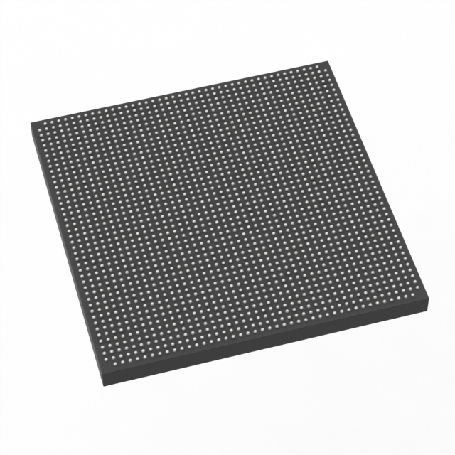
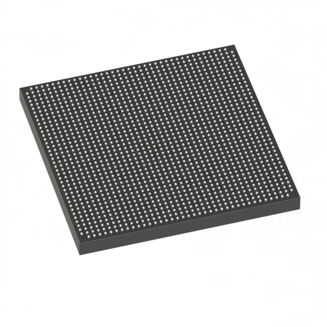
Stratix® V GX Field Programmable Gate Array (FPGA) IC 840 46080000 490000 1932-BBGA, FCBGA |
|---|---|
| Quantity | 681 Available (as of June 14, 2026) |

| Product Category | Field Programmable Gate Array (FPGA) |
|---|---|
| Manufacturer | Intel |
| Manufacturing Status | Obsolete |
| Manufacturer Standard Lead Time | Contact Us |
| Datasheet |
Specifications & Environmental
| Device Package | 1932-FBGA, FC (45x45) | Grade | Industrial | Operating Temperature | -40°C – 100°C | ||
|---|---|---|---|---|---|---|---|
| Package / Case | 1932-BBGA, FCBGA | Number of I/O | 840 | Voltage | 820 mV - 880 mV | ||
| Mounting Method | Surface Mount | RoHS Compliance | RoHS Compliant | REACH Compliance | REACH Unknown | ||
| Moisture Sensitivity Level | 3 (168 Hours) | Number of LABs/CLBs | 185000 | Number of Logic Elements/Cells | 490000 | ||
| Number of Gates | N/A | ECCN | 3A001A2C | HTS Code | 8542.39.0001 | ||
| Qualification | N/A | Total RAM Bits | 46080000 |
Overview of 5SGXMA5N2F45I3LN – Stratix® V GX FPGA, 490,000 logic elements, 840 I/O
The 5SGXMA5N2F45I3LN is a Stratix® V GX field-programmable gate array (FPGA) from Intel, offering a high-density programmable fabric in a 1932-BBGA FCBGA package. It combines large programmable logic resources, substantial embedded memory, and a high I/O count for demanding industrial applications.
With 490,000 logic elements and approximately 46 Mbits of embedded memory, this device targets designs that require extensive on-chip logic, significant on-chip RAM, and broad external interfacing while operating across an industrial temperature range.
Key Features
- Programmable Logic 490,000 logic elements provide extensive capacity for complex logic, state machines, and custom data-path implementations.
- Embedded Memory Approximately 46 Mbits of on-chip RAM for buffering, lookup tables, and intermediate storage without relying on external memory.
- I/O Density 840 I/O pins support large ensembles of external interfaces, sensors, and high-pin-count connectors.
- Package 1932-BBGA (1932-FBGA, 45×45) FCBGA package supports a high-pin-count, compact footprint for dense PCB designs.
- Power Core voltage supply range of 820 mV to 880 mV enables precise core power provisioning in system power architectures.
- Industrial Grade Temperature Rated for operation from −40 °C to 100 °C to meet industrial temperature requirements.
- Design Family Part of the Stratix V GX series, with electrical and switching characteristics documented in the Stratix V device datasheet for system-level integration.
Typical Applications
- Industrial control systems Industrial-grade temperature range and high I/O count enable field I/O aggregation, real-time control logic, and rugged deployment.
- High-density logic implementations Large logic element count and substantial embedded RAM allow integration of complex algorithms and large finite-state machines on-chip.
- I/O-intensive designs Up to 840 I/Os facilitate complex sensor arrays, multi-port connectivity, and large connector interfaces.
Unique Advantages
- High on-chip integration: 490,000 logic elements coupled with approximately 46 Mbits of embedded memory reduce dependence on external components.
- Robust industrial operation: Rated −40 °C to 100 °C for deployment in environments that require extended temperature tolerance.
- Extensive interfacing capability: 840 I/O pins provide flexibility for multi-channel designs and high-pin-count system interconnects.
- Compact high-density package: 1932-BBGA (45×45) delivers a dense pinout in a compact footprint for space-constrained boards.
- Deterministic core power range: Specified 820–880 mV core supply supports controlled power delivery and thermal planning.
- Documented device family: Stratix V GX series electrical and switching parameters are available in the Stratix V device datasheet for system integration reference.
Why Choose 5SGXMA5N2F45I3LN?
The 5SGXMA5N2F45I3LN balances high logic capacity, substantial embedded memory, and a very large I/O complement in a single industrial-grade FPGA package. Its combination of 490,000 logic elements, approximately 46 Mbits of on-chip RAM, and 840 I/Os makes it well-suited to designs that demand dense on-chip functionality and extensive external interfacing while operating across a wide temperature range.
This device is aimed at engineers designing complex programmable systems who require a proven Stratix V GX family architecture, predictable core-voltage specifications, and a high-density FCBGA package for compact, reliable board designs.
Request a quote or submit an inquiry to obtain pricing, availability, and ordering information for 5SGXMA5N2F45I3LN. Provide your design requirements and quantity to receive a tailored response.


Date Founded: 1968
Headquarters: Santa Clara, California, USA
Employees: 130,000+
Revenue: $54.23 Billion
Certifications and Memberships: ISO9001:2015, ISO14001:2015, ISO17025:2017, ISO27001:2022, ISO45001:2018, ISO50001:2018


