
5SGXMA7H2F35C1WN
| Part Description |
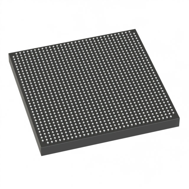
Stratix® V GX Field Programmable Gate Array (FPGA) IC 552 51200000 622000 1152-BBGA, FCBGA |
|---|---|
| Quantity | 1,284 Available (as of June 15, 2026) |

| Product Category | Field Programmable Gate Array (FPGA) |
|---|---|
| Manufacturer | Intel |
| Manufacturing Status | Obsolete |
| Manufacturer Standard Lead Time | Contact Us |
| Datasheet |
Specifications & Environmental
| Device Package | 1152-FBGA (35x35) | Grade | Commercial | Operating Temperature | 0°C – 85°C | ||
|---|---|---|---|---|---|---|---|
| Package / Case | 1152-BBGA, FCBGA | Number of I/O | 552 | Voltage | 870 mV - 930 mV | ||
| Mounting Method | Surface Mount | RoHS Compliance | RoHS non-compliant | REACH Compliance | REACH Unknown | ||
| Moisture Sensitivity Level | 4 (72 Hours) | Number of LABs/CLBs | 234720 | Number of Logic Elements/Cells | 622000 | ||
| Number of Gates | N/A | ECCN | OBSOLETE | HTS Code | N/A | ||
| Qualification | N/A | Total RAM Bits | 51200000 |
Overview of 5SGXMA7H2F35C1WN – Stratix® V GX Field Programmable Gate Array (FPGA) IC
The 5SGXMA7H2F35C1WN is a Stratix V GX family Field Programmable Gate Array (FPGA) in a high-density FCBGA package. It provides a large logic fabric, substantial on-chip memory, and a high I/O count, making it suited for designs that require dense programmable logic, significant embedded RAM, and extensive I/O connectivity.
Key Features
- Core Logic Provides 622,000 logic elements to implement complex digital functions and large custom logic networks.
- Embedded Memory Includes approximately 51.2 Mbits of embedded memory, enabling on-chip buffering, large LUT-based structures, and local data storage.
- I/O Capacity Features 552 user I/Os to support wide parallel interfaces and diverse peripheral connectivity.
- Package and Mounting Available in a 1152-BBGA FCBGA package (supplier package: 1152-FBGA, 35×35), optimized for surface-mount assembly in space-constrained designs.
- Power Core voltage supply specified between 870 mV and 930 mV, enabling designers to plan power delivery and regulation requirements precisely.
- Commercial Grade Temperature Rated for commercial operation from 0 °C to 85 °C, suitable for standard commercial and enterprise environments.
- Environmental Compliance RoHS-compliant construction to support regulatory and manufacturing requirements.
Typical Applications
- High-density logic designs Use the large logic element count for complex state machines, custom accelerators, and multi-function controllers.
- Memory-intensive processing Leverage approximately 51.2 Mbits of embedded RAM for buffering, packet processing, and intermediate data storage.
- I/O-centric systems Deploy in applications requiring many parallel or diverse interfaces, taking advantage of the 552 I/Os.
- Prototyping and system integration Ideal for validating large FPGA-based systems and integrating multiple subsystems on a single silicon device.
Unique Advantages
- High logic density: 622,000 logic elements let you consolidate functions that would otherwise require multiple devices, reducing board-level complexity.
- Substantial on-chip memory: Approximately 51.2 Mbits of embedded RAM supports large data buffers and local working memory without external SRAM/DRAM.
- Extensive I/O connectivity: 552 I/Os provide flexibility for high-pin-count interfaces and mixed-signal front-end connections.
- Compact ball-grid package: The 1152-BBGA FCBGA package offers a high pin count in a compact footprint to save PCB area.
- Commercial temperature rating: Specified 0 °C to 85 °C operation for reliable performance in standard commercial environments.
- Regulatory readiness: RoHS compliance supports environmentally conscious manufacturing and assembly processes.
Why Choose 5SGXMA7H2F35C1WN?
The 5SGXMA7H2F35C1WN delivers a balance of high logic capacity, sizable embedded memory, and broad I/O resources in a compact FCBGA package. Its commercial-grade rating and defined core voltage range make it suitable for enterprise and commercial embedded systems that demand dense programmable logic and substantial on-chip RAM.
This device is a strong fit for engineering teams building complex FPGA-based platforms that require integration, scalability, and predictable electrical characteristics. The combination of logic density, embedded memory, and I/O capability supports consolidation of functions and streamlined system designs.
Request a quote or submit a pricing inquiry today to get availability and ordering information for the 5SGXMA7H2F35C1WN.


Date Founded: 1968
Headquarters: Santa Clara, California, USA
Employees: 130,000+
Revenue: $54.23 Billion
Certifications and Memberships: ISO9001:2015, ISO14001:2015, ISO17025:2017, ISO27001:2022, ISO45001:2018, ISO50001:2018


