
5SGXMA7H2F35C1NCV
| Part Description |
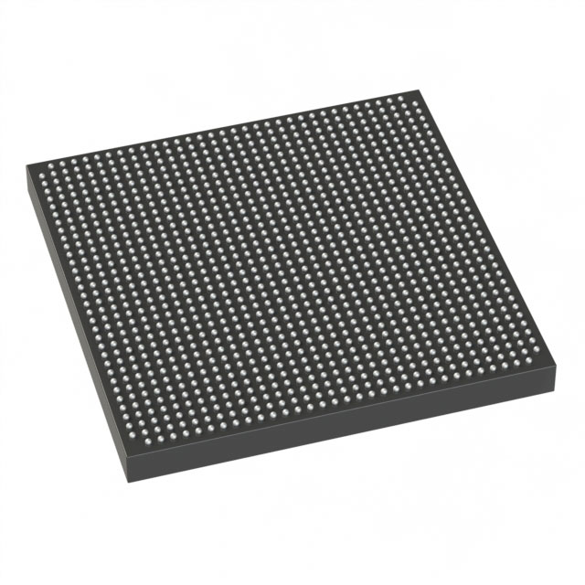
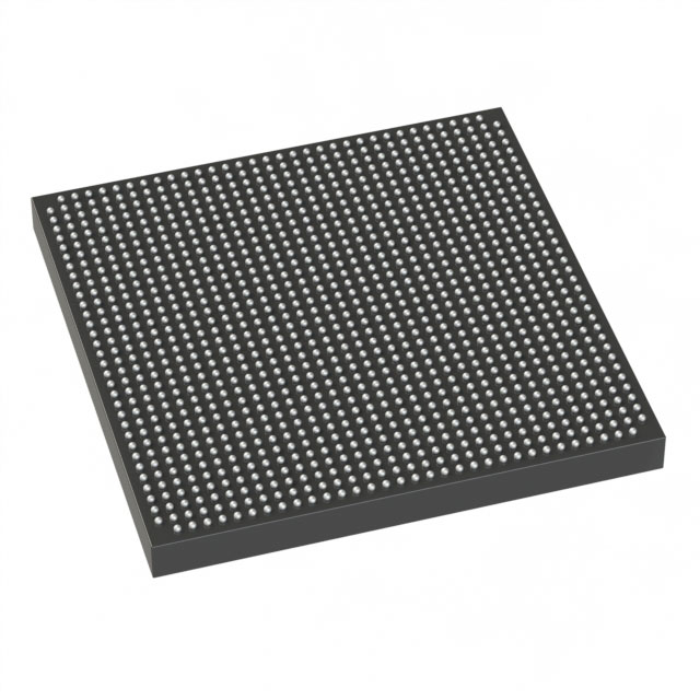
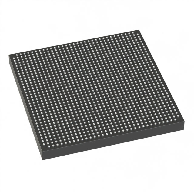
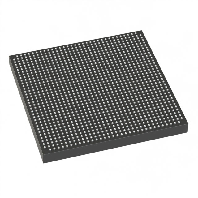
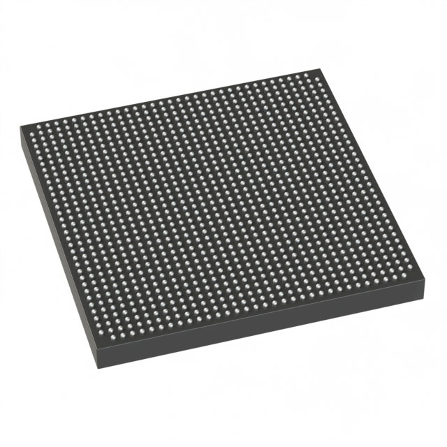
Stratix® V GX Field Programmable Gate Array (FPGA) IC 552 51200000 622000 1152-BBGA, FCBGA |
|---|---|
| Quantity | 374 Available (as of October 8, 2026) |
| Product Category | Field Programmable Gate Array (FPGA) |
|---|---|
| Manufacturer | Intel |
| Manufacturing Status | Obsolete |
| Manufacturer Standard Lead Time | Contact Us |
| Datasheet |
Specifications & Environmental
| Device Package | 1152-FBGA (35x35) | Grade | Commercial | Operating Temperature | 0°C – 85°C | ||
|---|---|---|---|---|---|---|---|
| Package / Case | 1152-BBGA, FCBGA | Number of I/O | 552 | Voltage | 870 mV - 930 mV | ||
| Mounting Method | Surface Mount | RoHS Compliance | RoHS non-compliant | REACH Compliance | REACH Unknown | ||
| Moisture Sensitivity Level | 4 (72 Hours) | Number of LABs/CLBs | 234720 | Number of Logic Elements/Cells | 622000 | ||
| Number of Gates | N/A | ECCN | OBSOLETE | HTS Code | N/A | ||
| Qualification | N/A | Total RAM Bits | 51200000 |
Overview of 5SGXMA7H2F35C1NCV – Stratix® V GX FPGA, 622,000 logic elements, ~51.2 Mbits RAM
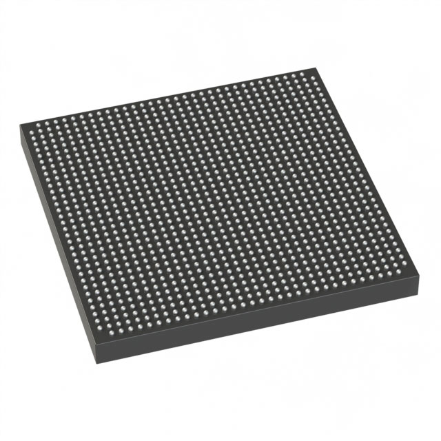
The 5SGXMA7H2F35C1NCV is a Stratix V GX field‑programmable gate array (FPGA) in a 1152‑BBGA FCBGA package. It delivers very high logic density together with substantial on‑chip RAM and a large I/O count for designs that require extensive programmable logic and memory resources.
Key attributes include approximately 51.2 Mbits of embedded memory, 622,000 logic elements, and 552 general‑purpose I/Os, making this device suitable for dense, high‑I/O designs implemented on surface‑mount PCBs within commercial temperature ranges.
Key Features
- Core Logic Density 622,000 logic elements for implementing large, complex digital designs and high‑capacity programmable logic.
- Embedded Memory Approximately 51.2 Mbits of on‑chip RAM to support large buffers, lookup tables, and state storage without immediate external memory dependencies.
- I/O Capacity 552 available I/Os to support extensive peripheral interfacing, multi‑lane connections, and high‑pin‑count board designs.
- Power Supply Core supply range specified from 870 mV to 930 mV to match system power rails and enable controlled power planning.
- Package and Mounting 1152‑BBGA (FCBGA); supplier device package shown as 1152‑FBGA (35×35). Surface‑mount mounting type for modern PCB assembly.
- Operating Range Commercial temperature grade with an operating range of 0 °C to 85 °C for standard commercial applications.
- Regulatory RoHS compliant to meet common environmental and manufacturing requirements.
Typical Applications
- High‑density digital processing Use the large logic element count to implement complex datapaths, algorithm accelerators, or multi‑core custom processors.
- Large on‑chip buffering Approximately 51.2 Mbits of embedded RAM supports large FIFO and buffering requirements for streaming or bursty data flows.
- High‑pin‑count I/O systems 552 I/Os enable integration with a broad set of peripherals, multi‑lane interfaces, and parallel sensor or actuator arrays.
- Surface‑mount board designs The 1152‑BBGA package and surface‑mount mounting type integrate with standard PCB assembly flows for compact, high‑performance boards.
Unique Advantages
- High logic capacity: 622,000 logic elements reduce the need for multiple FPGAs by consolidating complex functions into a single device.
- Substantial embedded memory: Approximately 51.2 Mbits of RAM lowers external memory requirements and simplifies board‑level RAM management.
- Extensive I/O availability: 552 I/Os provide flexibility for dense system interconnects and multiple peripheral interfaces without external expansion devices.
- Compact, production‑ready packaging: 1152‑BBGA (35×35) surface‑mount package supports high‑density board layouts and automated assembly.
- Commercial operating range: Rated 0 °C to 85 °C to match common commercial environments and deployments.
- RoHS compliant: Aligns with common manufacturing and environmental requirements for lead‑free production.
Why Choose 5SGXMA7H2F35C1NCV?
This Stratix V GX FPGA combines very high logic density, significant on‑chip RAM, and a large I/O complement in a single, surface‑mount BBGA package. It is positioned for designs that need to consolidate multiple functions into one programmable device while retaining ample embedded memory and I/O flexibility within a commercial temperature envelope.
Engineers and procurement teams that require scalable programmable logic capacity with robust memory resources will find this device suitable for advanced digital designs where board space, integration, and deterministic on‑chip resources matter.
Request a quote or contact sales to discuss availability, pricing, and delivery for the 5SGXMA7H2F35C1NCV FPGA.





















Date Founded: 1968
Headquarters: Santa Clara, California, USA
Employees: 130,000+
Revenue: $54.23 Billion
Certifications and Memberships: ISO9001:2015, ISO14001:2015, ISO17025:2017, ISO27001:2022, ISO45001:2018, ISO50001:2018


