
5SGXMA7K2F40I3N
| Part Description |
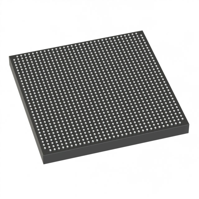
Stratix® V GX Field Programmable Gate Array (FPGA) IC 696 51200000 622000 1517-BBGA, FCBGA |
|---|---|
| Quantity | 328 Available (as of June 14, 2026) |

| Product Category | Field Programmable Gate Array (FPGA) |
|---|---|
| Manufacturer | Intel |
| Manufacturing Status | Obsolete |
| Manufacturer Standard Lead Time | Contact Us |
| Datasheet |
Specifications & Environmental
| Device Package | 1517-FBGA (40x40) | Grade | Industrial | Operating Temperature | -40°C – 100°C | ||
|---|---|---|---|---|---|---|---|
| Package / Case | 1517-BBGA, FCBGA | Number of I/O | 696 | Voltage | 820 mV - 880 mV | ||
| Mounting Method | Surface Mount | RoHS Compliance | RoHS Compliant | REACH Compliance | REACH Unknown | ||
| Moisture Sensitivity Level | 3 (168 Hours) | Number of LABs/CLBs | 234720 | Number of Logic Elements/Cells | 622000 | ||
| Number of Gates | N/A | ECCN | 3A001A2C | HTS Code | 8542.39.0001 | ||
| Qualification | N/A | Total RAM Bits | 51200000 |
Overview of 5SGXMA7K2F40I3N – Stratix V GX FPGA, 622,000 Logic Elements, 696 I/Os
The 5SGXMA7K2F40I3N is a Stratix® V GX Field Programmable Gate Array (FPGA) IC from Intel, offered in an industrial grade and packaged in a 1517-BBGA (FCBGA) format. This high-density FPGA integrates a large programmable fabric, abundant embedded memory, and extensive I/O to address designs requiring significant logic capacity and connectivity.
With 622,000 logic elements and approximately 51.2 Mbits of embedded memory, the device is targeted at I/O‑intensive, high‑density applications where on-chip resources and industrial temperature operation are important considerations.
Key Features
- Core Logic Approximately 622,000 logic elements provide substantial programmable fabric for implementing complex digital functions and custom processing pipelines.
- Embedded Memory Approximately 51.2 Mbits of on-chip RAM to support large buffers, FIFOs, and memory-hungry algorithms without external memory for some functions.
- I/O Density 696 user I/O pins deliver broad external connectivity for high-channel-count systems and dense board-level interfaces.
- Package & Mounting Supplied in a 1517-BBGA (FCBGA) package, supplier device package 1517-FBGA (40×40), designed for surface-mount assembly.
- Power Supply Core voltage supply range specified at 820 mV to 880 mV, enabling defined power-rail planning for the FPGA core.
- Operating Temperature Industrial temperature rating from −40 °C to 100 °C for deployment in temperature-challenging environments.
- RoHS Compliant Manufactured to meet RoHS requirements for environmental compliance.
Typical Applications
- High‑density digital processing Large logic element count and embedded memory make the device suitable for complex digital signal processing and algorithm acceleration.
- I/O‑intensive systems Extensive user I/Os support multi‑channel data aggregation, protocol bridging, and large peripheral arrays.
- Industrial equipment Industrial temperature rating and surface‑mount package align with embedded systems and control platforms operating across wide temperature ranges.
Unique Advantages
- Substantial on‑chip resources: 622,000 logic elements and ~51.2 Mbits of RAM reduce dependence on external logic and memory, simplifying BOM and board area.
- High connectivity: 696 I/Os allow flexible interfacing to sensors, transceivers, and high‑pin-count mezzanine modules without complex external multiplexing.
- Industrial readiness: Rated −40 °C to 100 °C to meet thermal requirements of industrial and ruggedized deployments.
- Compact, manufacturable package: 1517‑BBGA (FCBGA) surface‑mount package suited for automated assembly and high‑density PCB layouts.
- Defined core supply range: 820 mV to 880 mV specification supports precise power‑system design and voltage sequencing.
- Regulatory compliance: RoHS compliance supports environmental and regulatory requirements for many industries.
Why Choose 5SGXMA7K2F40I3N?
The 5SGXMA7K2F40I3N combines high logic density, substantial embedded memory, and broad I/O in a robust industrial‑grade Stratix V GX FPGA package. Its specification set supports design teams who need on‑chip capacity for complex processing, large data buffering, and extensive external interfacing while meeting industrial temperature requirements.
This device is appropriate for engineering teams focused on high‑performance, high‑integration designs that demand predictable electrical characteristics and manufacturable packaging. Its combination of resources provides a scalable foundation for long‑life projects where device capability and environmental tolerance are key selection criteria.
Request a quote or submit an inquiry to learn about availability and lead times for the 5SGXMA7K2F40I3N. Our team can provide pricing and ordering information to support your design and procurement process.


Date Founded: 1968
Headquarters: Santa Clara, California, USA
Employees: 130,000+
Revenue: $54.23 Billion
Certifications and Memberships: ISO9001:2015, ISO14001:2015, ISO17025:2017, ISO27001:2022, ISO45001:2018, ISO50001:2018


