
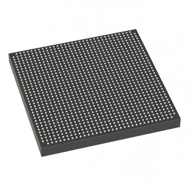
5SGXMA7K3F35C2LG
| Part Description |
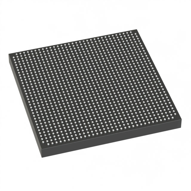
Stratix® V GX Field Programmable Gate Array (FPGA) IC 432 51200000 622000 1152-BBGA, FCBGA |
|---|---|
| Quantity | 1,266 Available (as of October 8, 2026) |
| Product Category | Field Programmable Gate Array (FPGA) |
|---|---|
| Manufacturer | Intel |
| Manufacturing Status | Active |
| Manufacturer Standard Lead Time | 26 Weeks |
| Datasheet |
Specifications & Environmental
| Device Package | 1152-FBGA (35x35) | Grade | Commercial | Operating Temperature | 0°C – 85°C | ||
|---|---|---|---|---|---|---|---|
| Package / Case | 1152-BBGA, FCBGA | Number of I/O | 432 | Voltage | 820 mV - 880 mV | ||
| Mounting Method | Surface Mount | RoHS Compliance | RoHS Compliant | REACH Compliance | REACH Unaffected | ||
| Moisture Sensitivity Level | 3 (168 Hours) | Number of LABs/CLBs | 234720 | Number of Logic Elements/Cells | 622000 | ||
| Number of Gates | N/A | ECCN | N/A | HTS Code | N/A | ||
| Qualification | N/A | Total RAM Bits | 51200000 |
Overview of 5SGXMA7K3F35C2LG – Stratix® V GX FPGA, 622,000 logic elements, ~51.2 Mbits embedded memory, 432 I/Os, 1152‑BBGA
The 5SGXMA7K3F35C2LG is a Stratix® V GX Field Programmable Gate Array (FPGA) IC offering high logic density and substantial on‑chip memory for commercial applications. Built for designs that require large programmable logic capacity, abundant I/O, and tight integration in a compact ball‑grid array package, this device targets embedded systems and communications equipment where commercial temperature operation and surface‑mount packaging are required.
Key Features
- Core Logic 622,000 logic elements for implementing complex custom logic, DSP, and control functions; includes 234,720 LABs for design partitioning and resource organization.
- Embedded Memory Approximately 51.2 Mbits of on‑chip RAM for buffering, packet processing, and state storage without external memory dependence.
- I/O Capability 432 user I/Os to support wide parallel interfaces, multiple high‑pin‑count peripherals, and flexible board routing.
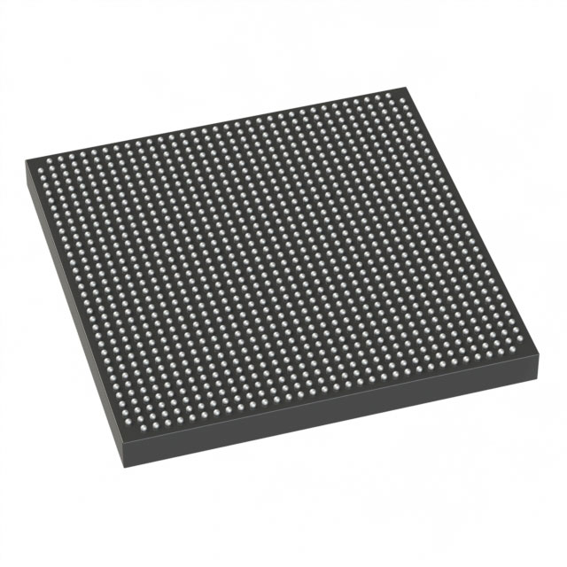
- Package & Mounting 1152‑BBGA (FCBGA) package; supplier device package listed as 1152‑FBGA (35×35). Surface mount package suitable for automated assembly.
- Power Core voltage supply range of 820 mV to 880 mV, enabling predictable power budgeting for core logic domains.
- Operating Grade & Temperature Commercial grade with an operating temperature range of 0 °C to 85 °C for standard commercial environments.
- Environmental Compliance RoHS compliant to meet common environmental and manufacturing requirements.
Typical Applications
- High‑density networking and communications — Use the device’s large logic capacity and abundant I/O to implement packet processing, protocol bridging, and custom switching logic in commercial networking equipment.
- Embedded compute and acceleration — Deploy as a programmable accelerator for compute‑intensive tasks where on‑chip RAM and high logic density reduce latency.
- Signal processing and DSP — Leverage the sizable embedded memory and logic resources for buffering and real‑time signal processing functions in commercial audio/video and instrumentation systems.
Unique Advantages
- High logic density: 622,000 logic elements enable extensive custom logic integration and complex system‑level functions on a single device.
- Substantial on‑chip memory: Approximately 51.2 Mbits of embedded RAM reduce reliance on external memory and simplify PCB design.
- Generous I/O count: 432 I/Os provide flexibility for multi‑lane interfaces, parallel buses, and diverse peripheral connectivity.
- Compact BGAs with surface‑mount compatibility: 1152‑BBGA / 1152‑FBGA (35×35) packaging allows high‑pin‑count integration in space‑constrained commercial boards.
- Predictable core power domain: 0.820–0.880 V core supply simplifies power rail planning for the FPGA core.
- Commercial temperature rating: Designed for standard commercial operating environments (0 °C to 85 °C), aligning with many consumer and enterprise applications.
Why Choose 5SGXMA7K3F35C2LG?
This Stratix V GX FPGA provides a balance of high logic capacity, significant embedded memory, and extensive I/O in a compact ball‑grid array package targeted at commercial applications. It is suitable for engineers and system designers who need to consolidate complex digital functions, large buffering requirements, and multiple interface endpoints into a single programmable device.
With RoHS compliance and a defined commercial operating range, the 5SGXMA7K3F35C2LG is positioned for deployments where predictable performance, integration density, and compliance matter. Its specification set supports scalable designs and system consolidation while fitting standard surface‑mount manufacturing flows.
Request a quote or submit an inquiry to get pricing and availability information for the 5SGXMA7K3F35C2LG and to discuss how it can fit into your next commercial FPGA design.





















Date Founded: 1968
Headquarters: Santa Clara, California, USA
Employees: 130,000+
Revenue: $54.23 Billion
Certifications and Memberships: ISO9001:2015, ISO14001:2015, ISO17025:2017, ISO27001:2022, ISO45001:2018, ISO50001:2018


