
5SGXMA7K3F40C2LN
| Part Description |
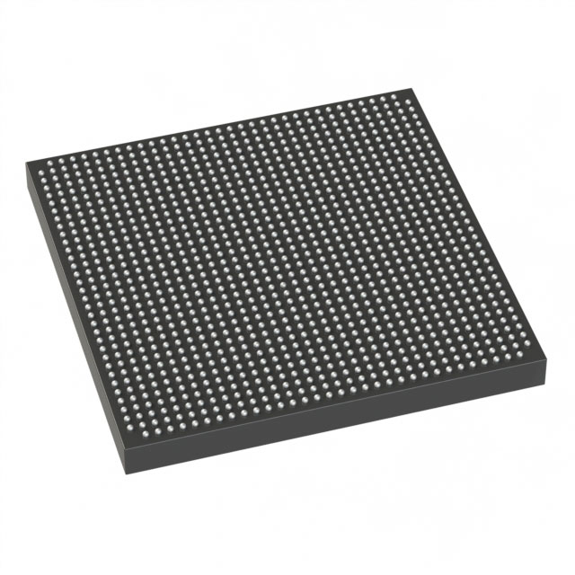
Stratix® V GX Field Programmable Gate Array (FPGA) IC 696 51200000 622000 1517-BBGA, FCBGA |
|---|---|
| Quantity | 528 Available (as of June 10, 2026) |

| Product Category | Field Programmable Gate Array (FPGA) |
|---|---|
| Manufacturer | Intel |
| Manufacturing Status | Obsolete |
| Manufacturer Standard Lead Time | Contact Us |
| Datasheet |
Specifications & Environmental
| Device Package | 1517-FBGA (40x40) | Grade | Commercial | Operating Temperature | 0°C – 85°C | ||
|---|---|---|---|---|---|---|---|
| Package / Case | 1517-BBGA, FCBGA | Number of I/O | 696 | Voltage | 820 mV - 880 mV | ||
| Mounting Method | Surface Mount | RoHS Compliance | RoHS Compliant | REACH Compliance | REACH Unknown | ||
| Moisture Sensitivity Level | 3 (168 Hours) | Number of LABs/CLBs | 234720 | Number of Logic Elements/Cells | 622000 | ||
| Number of Gates | N/A | ECCN | 3A001A2C | HTS Code | 8542.39.0001 | ||
| Qualification | N/A | Total RAM Bits | 51200000 |
Overview of 5SGXMA7K3F40C2LN – Stratix® V GX Field Programmable Gate Array (FPGA) IC, 622000 logic elements, ~51.2 Mbits RAM, 696 I/O, 1517-BBGA
The 5SGXMA7K3F40C2LN is a Stratix® V GX family FPGA from Intel (Altera) delivered in a 1517-BBGA FCBGA package. It provides a high logic capacity device architecture with extensive embedded memory and a large I/O count for demanding system-level designs.
With 622,000 logic elements and approximately 51.2 Mbits of on-chip RAM, this commercial-grade device targets applications that require dense logic integration, substantial embedded memory, and broad interface connectivity while operating within a commercial temperature range.
Key Features
- Core Logic 622,000 logic elements (cells) to implement complex digital designs and large-scale logic functions.
- Embedded Memory Approximately 51.2 Mbits of total on-chip RAM for buffering, LUT-based storage, and algorithm state storage.
- I/O Density 696 user I/O pins to support high-connectivity systems and multi-channel interfaces.
- Transceiver Family (Series-Level) Stratix V GX devices are documented in the series datasheet with GX transceiver speed-grade options (series-level information provided in the datasheet).
- Power Supply Core voltage supply range specified at 820 mV to 880 mV to match system power-rail design requirements.
- Package & Mounting 1517-BBGA FCBGA (supplier package listed as 1517-FBGA, 40×40) in a surface-mount form factor for board-level integration.
- Temperature & Grade Commercial-grade device with an operating temperature range of 0 °C to 85 °C.
- Compliance RoHS compliant.
Typical Applications
- High-density digital processing Use the large logic capacity and embedded memory for complex signal processing, algorithm acceleration, and custom compute tasks.
- Protocol aggregation and bridging Leverage the high I/O count to consolidate multiple interfaces and implement glue logic or protocol translation in system designs.
- Prototyping and system integration Deploy the device for board-level prototypes that require substantial on-chip resources and real-world I/O connectivity.
Unique Advantages
- High integration density: 622,000 logic elements and ~51.2 Mbits of embedded RAM reduce the need for external logic and memory components.
- Extensive I/O capacity: 696 I/O pins provide flexibility for multi-channel designs and parallel interfacing without external multiplexing.
- Compact, manufacturable package: 1517-BBGA FCBGA surface-mount package supports high-density PCB layouts and standard assembly processes.
- Controlled core voltage: Defined supply range (820 mV–880 mV) enables precise power delivery planning and thermal/power budgeting.
- Commercial temperature suitability: Rated for 0 °C to 85 °C operation to meet typical commercial electronics deployment requirements.
- Regulatory compliance: RoHS-compliant construction supports environmental and manufacturing requirements.
Why Choose 5SGXMA7K3F40C2LN?
The 5SGXMA7K3F40C2LN combines high logic capacity, substantial embedded memory, and a large I/O complement in a production-ready surface-mount BBGA package. Its specification set addresses designs requiring dense on-chip resources and broad interface connectivity while operating within a commercial temperature range and standardized power envelope.
This device is suited for engineering teams implementing complex digital systems, large custom accelerators, or multi-interface boards that benefit from consolidating logic and memory on a single FPGA platform backed by Intel (Altera) Stratix V series documentation.
Request a quote or submit an inquiry to obtain pricing, lead time, and availability for 5SGXMA7K3F40C2LN.


Date Founded: 1968
Headquarters: Santa Clara, California, USA
Employees: 130,000+
Revenue: $54.23 Billion
Certifications and Memberships: ISO9001:2015, ISO14001:2015, ISO17025:2017, ISO27001:2022, ISO45001:2018, ISO50001:2018


