
5SGXMA7N1F45I2G
| Part Description |
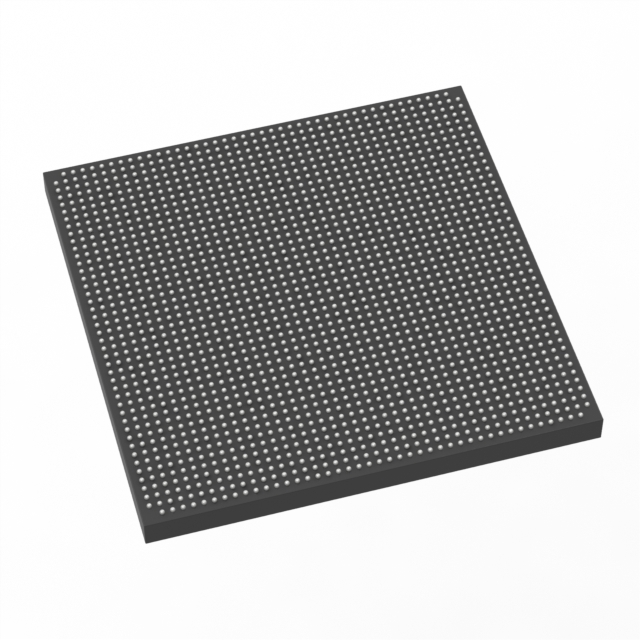
Stratix® V GX Field Programmable Gate Array (FPGA) IC 840 51200000 622000 1932-BBGA, FCBGA |
|---|---|
| Quantity | 230 Available (as of June 15, 2026) |

| Product Category | Field Programmable Gate Array (FPGA) |
|---|---|
| Manufacturer | Intel |
| Manufacturing Status | Active |
| Manufacturer Standard Lead Time | 26 Weeks |
| Datasheet |
Specifications & Environmental
| Device Package | 1932-FBGA, FC (45x45) | Grade | Industrial | Operating Temperature | -40°C – 100°C | ||
|---|---|---|---|---|---|---|---|
| Package / Case | 1932-BBGA, FCBGA | Number of I/O | 840 | Voltage | 870 mV - 930 mV | ||
| Mounting Method | Surface Mount | RoHS Compliance | RoHS Compliant | REACH Compliance | REACH Unaffected | ||
| Moisture Sensitivity Level | 3 (168 Hours) | Number of LABs/CLBs | 234720 | Number of Logic Elements/Cells | 622000 | ||
| Number of Gates | N/A | ECCN | N/A | HTS Code | N/A | ||
| Qualification | N/A | Total RAM Bits | 51200000 |
Overview of 5SGXMA7N1F45I2G – Stratix® V GX Field Programmable Gate Array (FPGA) IC
The 5SGXMA7N1F45I2G is an industrial-grade Stratix V GX field programmable gate array (FPGA) from Intel, delivered in a high-density 1932-BBGA FCBGA package. Designed for applications that require significant programmable logic, large embedded memory, and extensive I/O resources, this device supports demanding system designs in communications, high-performance embedded processing, and test/measurement equipment.
Key architectural highlights include approximately 622,000 logic elements, approximately 51.2 Mbits of on-chip RAM, and 840 I/O pins. The device operates across an industrial temperature range and uses a low-voltage supply domain appropriate to Stratix V core requirements.
Key Features
- Logic Capacity Approximately 622,000 logic elements for implementing large, complex digital designs and custom accelerators.
- Embedded Memory Approximately 51.2 Mbits of on-chip RAM to support large buffering, lookup tables, and state storage without external memory.
- I/O Density 840 programmable I/O pins to support broad peripheral connectivity, multi-lane interfaces, and system-level integration.
- High‑density Package 1932-BBGA (FCBGA) supplier package — 1932-FBGA, FC (45×45) — enabling compact board-level integration while providing high pin count.
- Power Supply Range Voltage supply specified at 870 mV to 930 mV, matching the device core operating window defined for Stratix V devices.
- Industrial Temperature Grade Rated for operation from −40 °C to 100 °C for deployment in industrial environments.
- Surface Mount Surface-mount device suitable for standard PCB assembly processes.
- Stratix V GX Family Transceiver Options Family-level documentation indicates GX channel options across multiple speed grades (for example, GX channel data rates up to 14.1 Gbps depending on speed grade).
- RoHS Compliant Build and materials conform to RoHS requirements.
Typical Applications
- High‑Performance Networking and Communications Implement packet processing, protocol offload, and interface bridging using the device’s large logic capacity and extensive I/O.
- Data Processing and Acceleration Custom hardware accelerators and streaming datapaths benefit from the combination of dense logic and substantial embedded RAM.
- Test, Measurement, and Instrumentation Complex signal processing, protocol emulation, and multi-channel I/O measurement systems leverage the device’s I/O count and industrial temperature rating.
- Embedded System Integration Consolidate multiple functions onto a single FPGA for system-level integration where on-chip memory and logic density reduce external component count.
Unique Advantages
- Large, Scalable Logic Resource: The device’s approximately 622,000 logic elements enable large designs and scalable implementations without immediate partitioning across multiple devices.
- Substantial On‑Chip Memory: Approximately 51.2 Mbits of embedded RAM reduce dependence on external memory for buffering and state retention, simplifying board-level design.
- High I/O Count: 840 I/O pins provide flexibility for multi‑lane interfaces, wide parallel buses, and dense peripheral connectivity.
- Industrial Reliability: Rated for −40 °C to 100 °C operation to meet industrial deployment temperature requirements.
- Compact High‑Pin Package: 1932‑ball FCBGA (45×45 mm) enables high pin count in a manageable PCB footprint for complex systems.
- Family-Level High‑Speed Transceiver Options: Stratix V GX family documentation details GX transceiver options across speed grades, offering designers choices for high-speed serial links where required.
Why Choose 5SGXMA7N1F45I2G?
The 5SGXMA7N1F45I2G positions itself as a high-density, industrial-grade Stratix V GX FPGA suitable for designs that require substantial programmable logic, on-chip RAM, and extensive I/O. Its combination of approximately 622,000 logic elements, about 51.2 Mbits of embedded memory, and 840 I/Os makes it a strong candidate for communications, data acceleration, and complex embedded systems where consolidation and integration matter.
Backed by Intel’s Stratix V family documentation and electrical specifications, this device offers designers a documented platform for building robust, high-capacity FPGA solutions that scale with design complexity and industrial operating requirements.
Request a quote or submit an inquiry to receive pricing, lead-time information, and technical support for the 5SGXMA7N1F45I2G.


Date Founded: 1968
Headquarters: Santa Clara, California, USA
Employees: 130,000+
Revenue: $54.23 Billion
Certifications and Memberships: ISO9001:2015, ISO14001:2015, ISO17025:2017, ISO27001:2022, ISO45001:2018, ISO50001:2018


