
5SGXMA7N1F45C2WN
| Part Description |
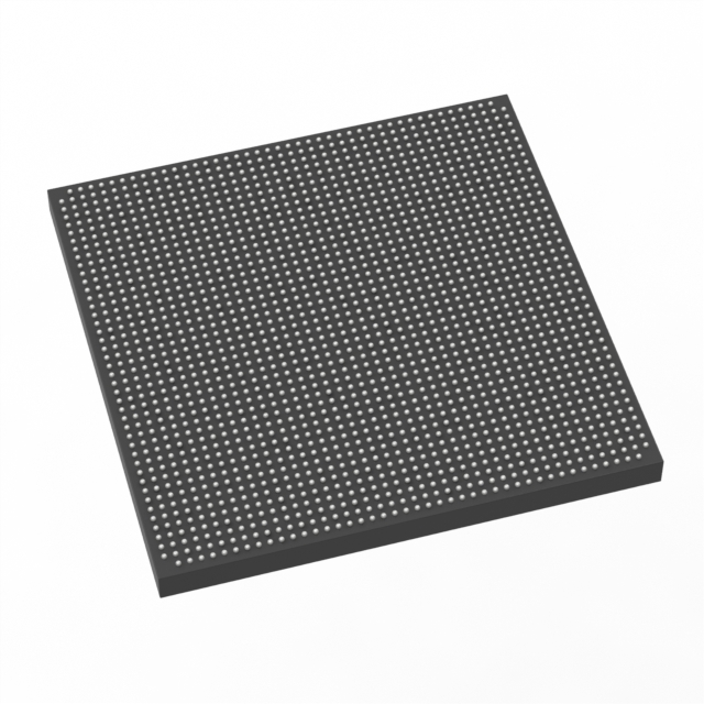
Stratix® V GX Field Programmable Gate Array (FPGA) IC 840 51200000 622000 1932-BBGA, FCBGA |
|---|---|
| Quantity | 831 Available (as of June 15, 2026) |

| Product Category | Field Programmable Gate Array (FPGA) |
|---|---|
| Manufacturer | Intel |
| Manufacturing Status | Obsolete |
| Manufacturer Standard Lead Time | Contact Us |
| Datasheet |
Specifications & Environmental
| Device Package | 1932-FBGA, FC (45x45) | Grade | Commercial | Operating Temperature | 0°C – 85°C | ||
|---|---|---|---|---|---|---|---|
| Package / Case | 1932-BBGA, FCBGA | Number of I/O | 840 | Voltage | 870 mV - 930 mV | ||
| Mounting Method | Surface Mount | RoHS Compliance | RoHS non-compliant | REACH Compliance | REACH Unknown | ||
| Moisture Sensitivity Level | 4 (72 Hours) | Number of LABs/CLBs | 234720 | Number of Logic Elements/Cells | 622000 | ||
| Number of Gates | N/A | ECCN | OBSOLETE | HTS Code | N/A | ||
| Qualification | N/A | Total RAM Bits | 51200000 |
Overview of 5SGXMA7N1F45C2WN – Stratix® V GX FPGA IC
The 5SGXMA7N1F45C2WN is a Stratix V GX field programmable gate array (FPGA) in a 1932-ball FCBGA package designed for commercial-grade applications. It provides a high density of programmable logic, embedded memory, and I/O to support complex digital systems where integration, board-level density, and configurability are required.
Key architectural highlights include 622,000 logic elements, approximately 51.2 Mbits of on-chip RAM, and up to 840 I/O pins, making this device suitable for designs that demand substantial logic capacity and large embedded memory within a compact surface-mount package.
Key Features
- Core Logic Capacity 622,000 logic elements for implementing large-scale digital designs and custom accelerators.
- Embedded Memory Approximately 51.2 Mbits of on-chip RAM to support buffering, FIFOs, and memory-intensive algorithms.
- I/O Density Up to 840 I/O pins to enable wide parallel interfaces and multi-channel connectivity.
- Package & Mounting Surface-mount 1932-BBGA (FCBGA) package; supplier device package listed as 1932-FBGA, FC (45×45) for compact board integration.
- Core Voltage Core supply range of 870 mV to 930 mV to match system power rails for core operation.
- Commercial Temperature Grade Rated for operation from 0 °C to 85 °C, suitable for commercial-environment deployments.
- Regulatory & Environmental RoHS compliant.
Typical Applications
- High-density digital processing Implement large custom logic blocks and datapaths using 622,000 logic elements and abundant embedded RAM.
- Memory-intensive algorithms Use approximately 51.2 Mbits of on-chip RAM for buffering, packet processing, or FPGA-based accelerators.
- Multi-channel I/O aggregation Deploy wide parallel interfaces or aggregate multiple serial/protocol channels using up to 840 I/Os.
- Compact board designs Integrate high logic and I/O density into space-constrained systems with the 1932-ball FCBGA surface-mount package.
Unique Advantages
- High logic scalability: 622,000 logic elements provide headroom for large state machines, datapaths, and custom processors without external logic.
- Significant on-chip RAM: Approximately 51.2 Mbits of embedded memory reduces the need for external memory for many buffering and algorithmic tasks.
- Extensive I/O count: Up to 840 I/Os enable complex board-level connectivity and interface consolidation.
- Compact, surface-mount packaging: The 1932-BBGA (FCBGA) package supports high-density PCB layouts while keeping the FPGA footprint efficient.
- Commercial temperature and RoHS compliance: Rated for 0 °C to 85 °C operation and RoHS compliant for standard commercial deployments.
- Low-voltage core operation: Core supply range of 870 mV to 930 mV aligns with modern low-voltage power designs.
Why Choose 5SGXMA7N1F45C2WN?
The 5SGXMA7N1F45C2WN combines very high logic density, substantial embedded RAM, and a large I/O count in a single commercial-grade, surface-mount FCBGA package. It is positioned for engineers and designers who need to consolidate complex digital functions onto a single FPGA while preserving board real estate and minimizing external memory and logic.
This device is a practical choice for commercial systems that require scalable programmable logic, abundant on-chip memory, and flexible I/O — delivered with RoHS compliance and defined operating and core-voltage ranges for predictable integration into your designs.
Request a quote or submit an inquiry to receive pricing, lead-time, and availability information for the 5SGXMA7N1F45C2WN.


Date Founded: 1968
Headquarters: Santa Clara, California, USA
Employees: 130,000+
Revenue: $54.23 Billion
Certifications and Memberships: ISO9001:2015, ISO14001:2015, ISO17025:2017, ISO27001:2022, ISO45001:2018, ISO50001:2018


