
5SGXMA7N2F40C1G
| Part Description |
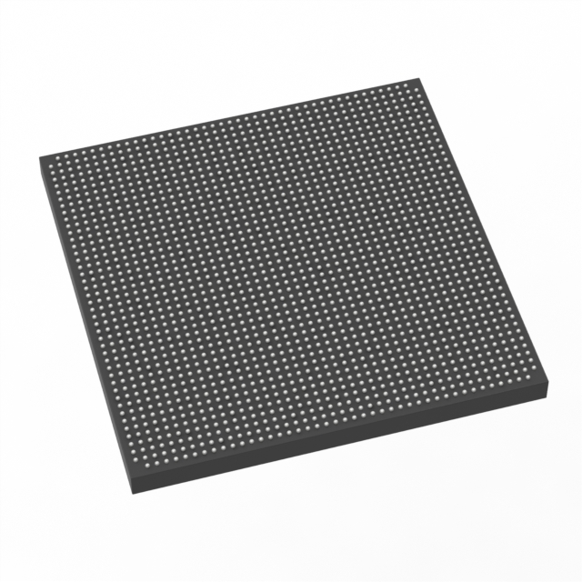
Stratix® V GX Field Programmable Gate Array (FPGA) IC 600 51200000 622000 1517-BBGA, FCBGA |
|---|---|
| Quantity | 163 Available (as of June 15, 2026) |

| Product Category | Field Programmable Gate Array (FPGA) |
|---|---|
| Manufacturer | Intel |
| Manufacturing Status | Active |
| Manufacturer Standard Lead Time | 26 Weeks |
| Datasheet |
Specifications & Environmental
| Device Package | 1517-FBGA (40x40) | Grade | Commercial | Operating Temperature | 0°C – 85°C | ||
|---|---|---|---|---|---|---|---|
| Package / Case | 1517-BBGA, FCBGA | Number of I/O | 600 | Voltage | 870 mV - 930 mV | ||
| Mounting Method | Surface Mount | RoHS Compliance | RoHS Compliant | REACH Compliance | REACH Unaffected | ||
| Moisture Sensitivity Level | 3 (168 Hours) | Number of LABs/CLBs | 234720 | Number of Logic Elements/Cells | 622000 | ||
| Number of Gates | N/A | ECCN | N/A | HTS Code | N/A | ||
| Qualification | N/A | Total RAM Bits | 51200000 |
Overview of 5SGXMA7N2F40C1G – Stratix V GX FPGA, 600 I/O, approximately 51.2 Mbits embedded memory, 622,000 logic elements
The 5SGXMA7N2F40C1G is an Intel Stratix® V GX field programmable gate array (FPGA) in a 1517-ball FCBGA package. It delivers very large programmable logic capacity, substantial on-chip embedded memory, and a high I/O count for demanding digital designs.
Engineered for high-density programmable logic applications, this commercial-grade device is suited to designs that require extensive logic resources, large memory buffers, and broad I/O connectivity while operating within a commercial temperature range.
Key Features
- Logic Capacity Provides 622,000 logic elements for implementing complex digital functions and large-scale logic designs.
- Embedded Memory Includes approximately 51.2 Mbits of on-chip RAM to support buffering, large FIFOs, and on-chip data storage.
- I/O Count 600 user I/O pins to support parallel interfaces, board-level connectivity, and system integration.
- Package and Mounting 1517-BBGA (FCBGA) package; supplier device package identified as 1517-FBGA (40×40). Surface-mount device suitable for standard PCB assembly flows.
- Power Supply Core voltage supply range of 870 mV to 930 mV as specified for the device.
- Operating Grade and Temperature Commercial grade with an operating temperature range of 0 °C to 85 °C.
- Compliance RoHS compliant.
- Family-Level Electrical and Transceiver Information Device is part of the Stratix V GX family; the Stratix V device datasheet details electrical and switching characteristics and lists available transceiver and core speed grades.
Typical Applications
- Complex digital prototyping Large logic capacity and ample embedded memory enable rapid implementation of system-level prototypes and FPGA-based development platforms.
- High-density I/O subsystems With 600 I/Os, the device supports dense board-level connectivity for multi-channel interfaces and parallel peripheral integration.
- Data buffering and on-chip storage Approximately 51.2 Mbits of embedded RAM supports large FIFOs, buffering, and intermediate data storage for signal processing pipelines.
Unique Advantages
- Extensive logic resources: 622,000 logic elements enable implementation of large, complex designs without immediate partitioning across multiple devices.
- Substantial on-chip memory: Approximately 51.2 Mbits of embedded RAM reduces reliance on external memory for many buffering and data management tasks.
- High I/O flexibility: 600 I/Os provide broad connectivity for complex boards and multi-channel interfaces, simplifying system integration.
- Commercial temperature rating: Designed for commercial applications with specified 0 °C to 85 °C operating range and commercial-grade speed options.
- Industry-standard package: 1517-ball FCBGA (40×40) surface-mount package supports conventional assembly and board designs.
- Regulatory compliance: RoHS compliance supports environmental and manufacturing requirements.
Why Choose 5SGXMA7N2F40C1G?
The 5SGXMA7N2F40C1G provides a combination of very large logic capacity, significant embedded memory, and a high I/O count in a commercial-grade Stratix V GX FPGA. These characteristics make it a strong candidate for designs that consolidate complex logic, buffering, and wide connectivity into a single programmable device.
Engineers designing high-density digital systems will find the device’s resource balance useful for scaling prototypes and production designs while relying on Intel's Stratix V family documentation for detailed electrical, switching, and transceiver-grade information.
Request a quote or submit an inquiry to receive pricing, availability, and further technical support for the 5SGXMA7N2F40C1G.


Date Founded: 1968
Headquarters: Santa Clara, California, USA
Employees: 130,000+
Revenue: $54.23 Billion
Certifications and Memberships: ISO9001:2015, ISO14001:2015, ISO17025:2017, ISO27001:2022, ISO45001:2018, ISO50001:2018


