
5SGXMA7N3F45C3G
| Part Description |
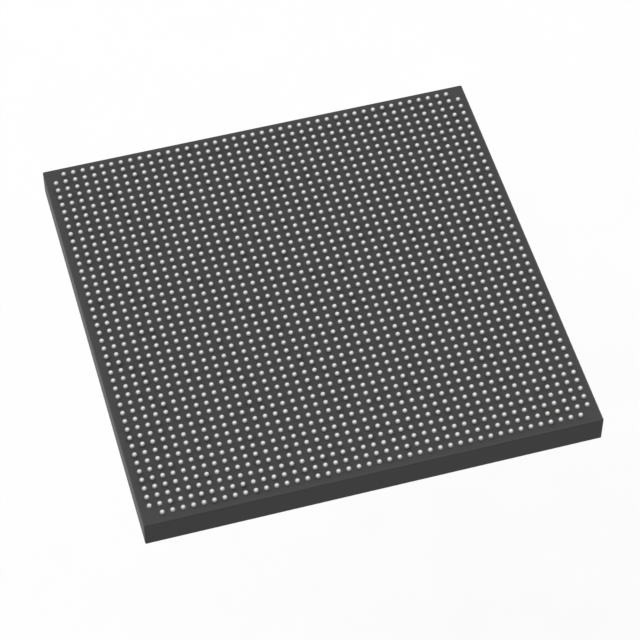
Stratix® V GX Field Programmable Gate Array (FPGA) IC 840 51200000 622000 1932-BBGA, FCBGA |
|---|---|
| Quantity | 1,217 Available (as of June 14, 2026) |

| Product Category | Field Programmable Gate Array (FPGA) |
|---|---|
| Manufacturer | Intel |
| Manufacturing Status | Active |
| Manufacturer Standard Lead Time | 26 Weeks |
| Datasheet |
Specifications & Environmental
| Device Package | 1932-FBGA, FC (45x45) | Grade | Commercial | Operating Temperature | 0°C – 85°C | ||
|---|---|---|---|---|---|---|---|
| Package / Case | 1932-BBGA, FCBGA | Number of I/O | 840 | Voltage | 820 mV - 880 mV | ||
| Mounting Method | Surface Mount | RoHS Compliance | RoHS Compliant | REACH Compliance | REACH Unaffected | ||
| Moisture Sensitivity Level | 3 (168 Hours) | Number of LABs/CLBs | 234720 | Number of Logic Elements/Cells | 622000 | ||
| Number of Gates | N/A | ECCN | N/A | HTS Code | N/A | ||
| Qualification | N/A | Total RAM Bits | 51200000 |
Overview of 5SGXMA7N3F45C3G – Stratix® V GX FPGA, 840 I/O, 622,000 Logic Elements
The 5SGXMA7N3F45C3G is a Stratix® V GX Field Programmable Gate Array (FPGA) from Intel, delivered in a 1932-BBGA FCBGA package for surface-mount assembly. It provides a high logic capacity and substantial embedded memory with a large I/O count, targeting designs that require dense programmable logic, significant on-chip RAM, and extensive connectivity within commercial-temperature environments.
Designed for commercial-grade deployments, this FPGA operates across a 0 °C to 85 °C range and is RoHS compliant. Core supply voltage is specified between 820 mV and 880 mV, enabling use in systems designed around low-voltage FPGA cores.
Key Features
- Core FPGA Architecture Stratix V GX family device offering high-density programmable logic in an FPGA form factor.
- Logic Capacity 622,000 logic elements to support complex digital designs and large-scale integration.
- Embedded Memory Approximately 51.2 Mbits of on-chip RAM for data buffering, caches, and scratchpad memory.
- I/O Density 840 user I/O pins to simplify external interfacing and system-level connectivity.
- Power Core voltage supply range: 820 mV to 880 mV (0.82–0.88 V) for the device core.
- Package & Mounting 1932-BBGA, FCBGA package (supplier designation: 1932-FBGA, FC (45×45)); surface-mount device.
- Operating Conditions Commercial temperature grade with operating range 0 °C to 85 °C.
- Compliance RoHS compliant.
- Family-Level Transceiver Options Stratix V GX family devices are documented with multiple transceiver and core speed grade offerings in the device datasheet.
Typical Applications
- High-density digital processing — Use the large logic capacity and on-chip RAM for complex signal processing, algorithm acceleration, or custom compute engines.
- I/O-intensive systems — The 840 available I/Os enable rich peripheral interfacing and multi-channel data aggregation without immediate need for external IO expanders.
- Memory-dependent designs — Approximately 51.2 Mbits of embedded memory supports buffering, packet handling, and intermediate data storage.
- Advanced prototyping and integration — Surface-mount 1932-BBGA packaging and commercial temperature rating make the device suitable for development platforms and production systems in commercial environments.
Unique Advantages
- High integration density: 622,000 logic elements reduce the need for multiple discrete devices and lower overall system BOM complexity.
- Large on-chip memory: Approximately 51.2 Mbits of embedded RAM minimizes reliance on external memory for many buffering and scratchpad use cases.
- Extensive I/O: 840 I/O pins simplify system connectivity and reduce external I/O components.
- Commercial-grade readiness: Rated for 0 °C to 85 °C operation for mainstream embedded and communications equipment.
- Surface-mount BGA package: 1932-BBGA (45×45) supports high pin-count routing density in compact board layouts.
- Standards-compliant manufacturing: RoHS compliance supports environmental and regulatory requirements for commercial products.
Why Choose 5SGXMA7N3F45C3G?
The 5SGXMA7N3F45C3G brings together a high logic element count, substantial on-chip RAM, and a large I/O complement in a commercial-grade Stratix V GX FPGA. Its package and electrical characteristics make it suitable for designers who need to consolidate logic, memory, and connectivity into a single programmable device while meeting standard commercial operating conditions.
As part of the Intel Stratix V GX family and backed by the published device datasheet, this FPGA is appropriate for teams building scalable, high-density systems where integration and clear device specifications are key to design confidence.
Request a quote or submit your specifications to receive pricing and availability for the 5SGXMA7N3F45C3G. Our team will respond with lead-time and ordering information to help move your design forward.


Date Founded: 1968
Headquarters: Santa Clara, California, USA
Employees: 130,000+
Revenue: $54.23 Billion
Certifications and Memberships: ISO9001:2015, ISO14001:2015, ISO17025:2017, ISO27001:2022, ISO45001:2018, ISO50001:2018


