
5SGXMA9N1F45C2LN
| Part Description |
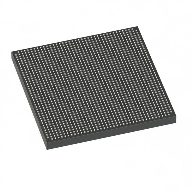
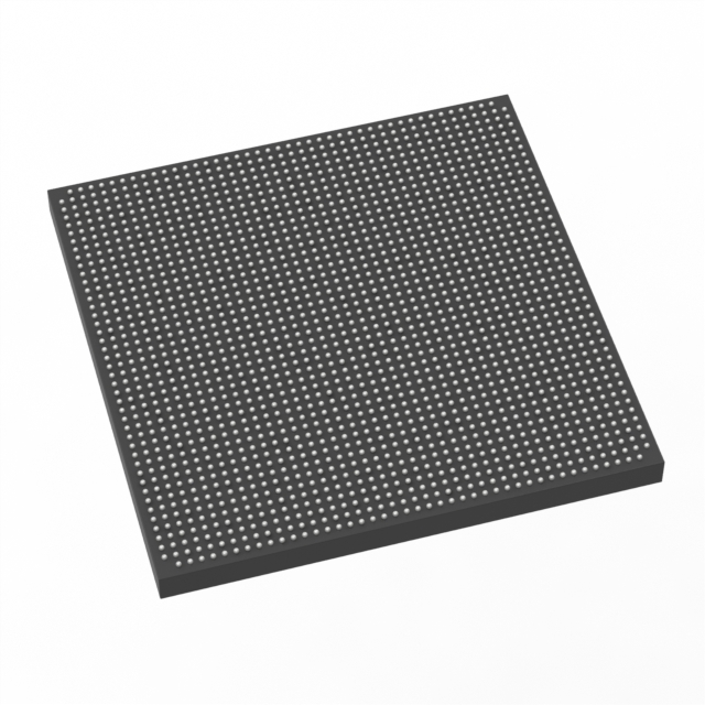
Stratix® V GX Field Programmable Gate Array (FPGA) IC 840 53248000 840000 1932-BBGA, FCBGA |
|---|---|
| Quantity | 699 Available (as of June 18, 2026) |

| Product Category | Field Programmable Gate Array (FPGA) |
|---|---|
| Manufacturer | Intel |
| Manufacturing Status | Obsolete |
| Manufacturer Standard Lead Time | Contact Us |
| Datasheet |
Specifications & Environmental
| Device Package | 1932-FBGA, FC (45x45) | Grade | Commercial | Operating Temperature | 0°C – 85°C | ||
|---|---|---|---|---|---|---|---|
| Package / Case | 1932-BBGA, FCBGA | Number of I/O | 840 | Voltage | 820 mV - 880 mV | ||
| Mounting Method | Surface Mount | RoHS Compliance | RoHS Compliant | REACH Compliance | REACH Unknown | ||
| Moisture Sensitivity Level | 3 (168 Hours) | Number of LABs/CLBs | 317000 | Number of Logic Elements/Cells | 840000 | ||
| Number of Gates | N/A | ECCN | 3A001A2C | HTS Code | 8542.39.0001 | ||
| Qualification | N/A | Total RAM Bits | 53248000 |
Overview of 5SGXMA9N1F45C2LN – Stratix® V GX FPGA, 840K Logic Elements, 1932-BBGA
The 5SGXMA9N1F45C2LN is a Stratix V GX field programmable gate array (FPGA) IC from Intel, offered as a commercial-grade device. It provides large on-chip logic and memory capacity along with a high I/O count in a 1932‑ball FCBGA package, making it suited for designs that require substantial programmable logic, embedded memory, and dense external interfacing.
Key capabilities include 840,000 logic elements, approximately 53 Mbits of embedded memory, and 840 I/O pins, combined with a low-voltage core supply range and commercial temperature grading for mainstream high‑performance applications.
Key Features
- Core Architecture Stratix V GX family FPGA architecture in a Stratix V device form factor optimized for large logic designs.
- Logic Capacity 840,000 logic elements (cells) to implement complex state machines, datapaths, and custom hardware accelerators.
- Embedded Memory Approximately 53 Mbits of on-chip RAM to support large buffers, FIFOs, and local data storage.
- I/O Density 840 I/O pins for extensive external connectivity and high pin-count system integration.
- Power and Core Supply Core voltage supply range: 820 mV to 880 mV, enabling targeted core-voltage provisioning for this device.
- Package & Mounting 1932‑BBGA (FCBGA) package; Supplier device package: 1932‑FBGA, FC (45×45). Surface‑mount mounting type for modern PCB assembly.
- Commercial Temperature Grade Rated for operation from 0 °C to 85 °C for commercial applications.
- Environmental Compliance RoHS compliant to support lead‑free manufacturing and regulatory requirements.
Typical Applications
- Network and Telecom Systems Use the device where large logic capacity and high I/O count are needed to implement packet processing, protocol parsing, or interface consolidation.
- Data Path Acceleration Implement custom accelerators, encryption/decryption engines, and high-throughput datapaths leveraging abundant logic and embedded RAM.
- High‑Density I/O Systems Consolidate multiple peripherals and interfaces in a single FPGA where a large number of I/Os simplifies board-level design.
- Prototyping and Complex SoC Integration Integrate substantial programmable logic and memory to prototype silicon, verify algorithms, or offload functions from a host processor.
Unique Advantages
- Substantial Logic Resources: 840,000 logic elements enable large-scale hardware designs without immediate need for multiple devices.
- Significant On‑Chip Memory: Approximately 53 Mbits of embedded RAM reduce external memory dependence and improve data locality and throughput.
- High I/O Count: 840 I/Os allow direct interfacing to numerous peripherals, PHYs, and high-pin-count connectors, simplifying system routing.
- Compact, Surface‑Mount Package: 1932‑BBGA (45×45) package offers high pin density in a board-mountable form factor for space-constrained systems.
- Commercial Grade Reliability: Designed and specified for commercial temperature ranges (0 °C to 85 °C) and RoHS compliance for mainstream production.
- Controlled Core Supply Range: Narrow core voltage window (820 mV to 880 mV) supports consistent power delivery and predictable core performance.
Why Choose 5SGXMA9N1F45C2LN?
The 5SGXMA9N1F45C2LN is positioned for engineers and teams that need a highly capable Stratix V GX FPGA with a substantial mix of logic, embedded RAM, and I/O in a single commercial‑grade package. Its combination of 840,000 logic elements, approximately 53 Mbits of on‑chip memory, and 840 I/Os offers a balanced platform for complex hardware acceleration, protocol processing, and high‑density system integration.
Choosing this FPGA can reduce system complexity by consolidating multiple functions into one device, maintain a compact PCB footprint with its 1932‑BBGA surface‑mount package, and support production deployments within standard commercial operating temperatures and RoHS requirements.
Request a quote or submit an inquiry to obtain pricing and availability for the 5SGXMA9N1F45C2LN. Our team will respond with product lead times and ordering information.


Date Founded: 1968
Headquarters: Santa Clara, California, USA
Employees: 130,000+
Revenue: $54.23 Billion
Certifications and Memberships: ISO9001:2015, ISO14001:2015, ISO17025:2017, ISO27001:2022, ISO45001:2018, ISO50001:2018


