
5SGXMA9N1F45C2G
| Part Description |
Stratix® V GX Field Programmable Gate Array (FPGA) IC 840 53248000 840000 1932-BBGA, FCBGA |
|---|---|
| Quantity | 547 Available (as of June 15, 2026) |

| Product Category | Field Programmable Gate Array (FPGA) |
|---|---|
| Manufacturer | Intel |
| Manufacturing Status | Active |
| Manufacturer Standard Lead Time | 26 Weeks |
| Datasheet |
Specifications & Environmental
| Device Package | 1932-FBGA, FC (45x45) | Grade | Commercial | Operating Temperature | 0°C – 85°C | ||
|---|---|---|---|---|---|---|---|
| Package / Case | 1932-BBGA, FCBGA | Number of I/O | 840 | Voltage | 870 mV - 930 mV | ||
| Mounting Method | Surface Mount | RoHS Compliance | RoHS Compliant | REACH Compliance | REACH Unaffected | ||
| Moisture Sensitivity Level | 3 (168 Hours) | Number of LABs/CLBs | 317000 | Number of Logic Elements/Cells | 840000 | ||
| Number of Gates | N/A | ECCN | N/A | HTS Code | N/A | ||
| Qualification | N/A | Total RAM Bits | 53248000 |
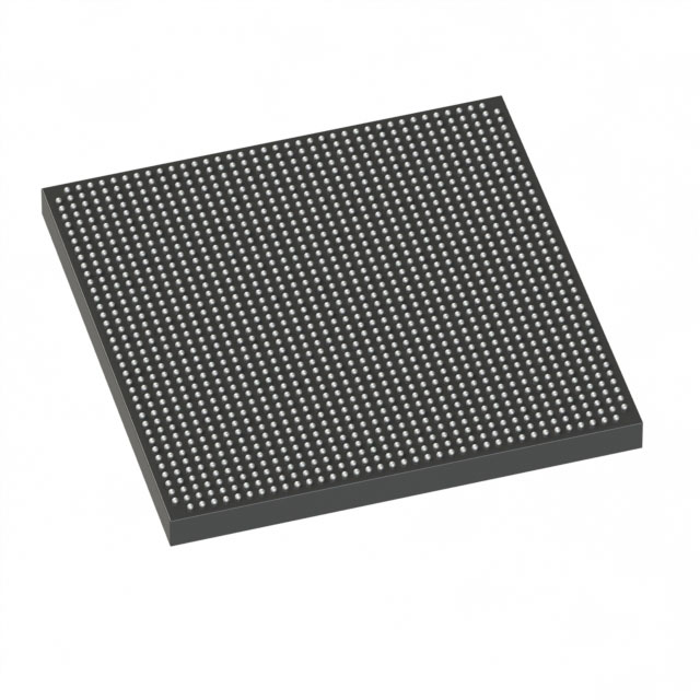
Overview of 5SGXMA9N1F45C2G – Stratix® V GX FPGA IC, 840,000 logic elements, 1932-BBGA
The 5SGXMA9N1F45C2G is a Stratix V GX field-programmable gate array (FPGA) IC from Intel, designed for high-density, programmable logic implementations. This commercial-grade device combines a large logic fabric with substantial embedded memory and extensive I/O, delivered in a 1932-ball BGA (FCBGA) package for surface-mount assembly.
Engineered as part of the Stratix V GX family, the device targets applications requiring a dense mix of logic, on-chip RAM, and high channel I/O counts while operating within a core supply range of 870 mV to 930 mV and a commercial temperature range of 0 °C to 85 °C.
Key Features
- Core Logic 840,000 logic elements for complex programmable logic and high gate-count designs.
- Embedded Memory Approximately 53 Mbits of on-chip RAM to support large buffering, state storage, and memory-intensive functions.
- I/O Density 840 user I/O pins, enabling extensive external interfacing and parallel connectivity.
- Power Core voltage supply specified from 870 mV to 930 mV for the device core.
- Package & Mounting 1932-BBGA (FCBGA) package; supplier device package listed as 1932-FBGA, FC (45×45). Surface-mount footprint.
- Operating Grade & Temperature Commercial grade with an operating temperature range of 0 °C to 85 °C.
- Compliance RoHS compliant.
- Stratix V GX Family Characteristics As a Stratix V GX device, the family-level documentation describes transceiver speed-grade options; consult the device datasheet for transceiver and switching characteristics applicable to specific speed grades.
Typical Applications
- High-density logic implementations Leverage 840,000 logic elements and approximately 53 Mbits of embedded memory for complex state machines, datapath logic, and custom accelerators.
- Multi‑I/O systems High I/O count (840 pins) supports broad interfacing requirements for parallel peripherals, mezzanine modules, and high-pin-count daughtercards.
- High-speed serial / communications (family-level) Stratix V GX family documentation includes transceiver speed-grade options for multi-gigabit channels; refer to the datasheet for applicable transceiver capabilities by speed grade.
Unique Advantages
- Large programmable fabric: 840,000 logic elements provide substantial capacity for large-scale digital designs and complex algorithm implementation.
- Significant embedded memory: Approximately 53 Mbits of on-chip RAM reduces external memory dependence and simplifies board-level memory architectures.
- Extensive connectivity: 840 I/Os enable flexible system partitioning and support for dense peripheral and interface requirements.
- Commercial temperature suitability: Rated for 0 °C to 85 °C operation, appropriate for a wide range of commercial and enterprise applications.
- Surface-mount FCBGA packaging: 1932-ball FCBGA (45×45) offers a compact, high-pin-count solution for modern PCB assemblies.
- Standards-compliant material set: RoHS compliance supports regulatory and manufacturing requirements for lead-free production.
Why Choose 5SGXMA9N1F45C2G?
The 5SGXMA9N1F45C2G brings together a high-count programmable fabric, substantial embedded memory, and broad I/O in a single, commercial-grade Stratix V GX FPGA package. Its specification set supports designs that require large logic capacity and on-chip memory while operating within a defined core voltage window and a commercial temperature range.
Designers seeking a high-density, programmable solution with family-level Stratix V GX transceiver capabilities and a compact FCBGA footprint can rely on the documented electrical and switching characteristics provided in the Stratix V device documentation for integration and system-level planning.
Request a quote or submit an inquiry to receive pricing, lead time, and availability details for the 5SGXMA9N1F45C2G.


Date Founded: 1968
Headquarters: Santa Clara, California, USA
Employees: 130,000+
Revenue: $54.23 Billion
Certifications and Memberships: ISO9001:2015, ISO14001:2015, ISO17025:2017, ISO27001:2022, ISO45001:2018, ISO50001:2018


