
5SGXMA9N3F45C3N
| Part Description |
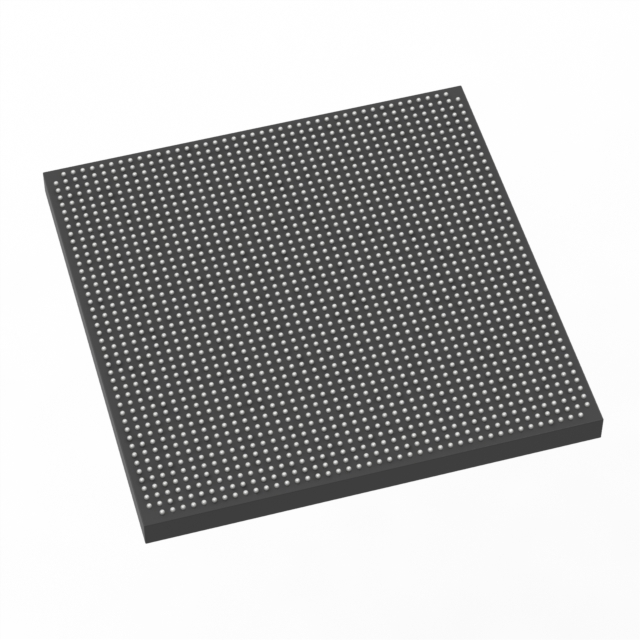
Stratix® V GX Field Programmable Gate Array (FPGA) IC 840 53248000 840000 1932-BBGA, FCBGA |
|---|---|
| Quantity | 837 Available (as of June 15, 2026) |

| Product Category | Field Programmable Gate Array (FPGA) |
|---|---|
| Manufacturer | Intel |
| Manufacturing Status | Obsolete |
| Manufacturer Standard Lead Time | Contact Us |
| Datasheet |
Specifications & Environmental
| Device Package | 1932-FBGA, FC (45x45) | Grade | Commercial | Operating Temperature | 0°C – 85°C | ||
|---|---|---|---|---|---|---|---|
| Package / Case | 1932-BBGA, FCBGA | Number of I/O | 840 | Voltage | 820 mV - 880 mV | ||
| Mounting Method | Surface Mount | RoHS Compliance | RoHS Compliant | REACH Compliance | REACH Unknown | ||
| Moisture Sensitivity Level | 3 (168 Hours) | Number of LABs/CLBs | 317000 | Number of Logic Elements/Cells | 840000 | ||
| Number of Gates | N/A | ECCN | 3A001A2C | HTS Code | 8542.39.0001 | ||
| Qualification | N/A | Total RAM Bits | 53248000 |
Overview of 5SGXMA9N3F45C3N – Stratix® V GX Field Programmable Gate Array (FPGA)
The 5SGXMA9N3F45C3N is a high-density Stratix® V GX FPGA from Intel, offering 840,000 logic elements and approximately 53 Mbits of embedded memory. Built in a high-pin-count 1932-BBGA (1932-FBGA, FC 45×45) package with up to 840 I/O, this surface-mount commercial-grade device suits complex, I/O‑intensive programmable designs.
Its supported core supply range of 820 mV to 880 mV and commercial operating temperature range of 0 °C to 85 °C provide clear electrical and thermal boundaries for system integration. The device is RoHS compliant.
Key Features
- Core Logic 840,000 logic elements provide large programmable logic capacity for complex algorithms and parallel processing tasks.
- Embedded Memory Approximately 53 Mbits of on-chip RAM for buffering, state storage, and memory-intensive logic functions.
- I/O Density Up to 840 user I/O pins to support high‑channel-count interfaces, broad peripheral connectivity, and system-level integration.
- Package & Mounting 1932-BBGA (supplier package: 1932-FBGA, FC 45×45) in a surface‑mount ball‑grid array for high pin count and compact board-level integration.
- Power Supply Core voltage specified between 820 mV and 880 mV to match regulated power rails and power‑delivery planning.
- Commercial Temperature Grade Rated for operation from 0 °C to 85 °C, suitable for commercial temperature environments and standard electronics applications.
- Standards Compliance RoHS compliant to support environmental and regulatory requirements.
Typical Applications
- High‑density digital processing Designs requiring large programmable logic and embedded RAM capacity for custom signal processing and algorithm acceleration.
- High‑pin-count interface aggregation Systems that need many I/Os for multi‑lane data aggregation, protocol bridging, or extensive sensor and peripheral connectivity.
- Platform and prototyping Complex FPGA platforms and reference designs where high logic count and on‑chip memory enable rapid development and system validation.
Unique Advantages
- Extensive programmable capacity: 840,000 logic elements support large-scale designs without immediate need for multi‑FPGA partitioning.
- Substantial embedded memory: Approximately 53 Mbits of RAM reduces external memory dependency for many buffering and storage tasks.
- Very high I/O count: Up to 840 I/O pins simplify board-level routing for dense interface requirements and reduce the need for additional interface chips.
- Compact, high‑pin package: The 1932‑ball BGA (45×45 FC footprint) concentrates I/O and silicon area for space-constrained, high‑performance designs.
- Clear electrical envelope: Defined core supply range (820–880 mV) aids power-supply design and system integration planning.
- Commercial-grade readiness: Rated 0 °C to 85 °C for applications targeting commercial temperature specifications.
Why Choose 5SGXMA9N3F45C3N?
The 5SGXMA9N3F45C3N positions itself as a high‑density Stratix® V GX FPGA for projects that demand a large logic fabric, significant on‑chip memory, and a very high I/O count in a single‑device solution. Its package and electrical specifications make it suitable for integration into complex commercial systems where board space and interface density are key considerations.
For engineering teams and procurement groups looking for a programmable silicon option with clear electrical and thermal limits, this device offers scalability for advanced designs while simplifying component selection through its consolidated logic, memory, and I/O capabilities.
Request a quote or submit your inquiry to receive pricing, availability, and lead‑time information for the 5SGXMA9N3F45C3N.


Date Founded: 1968
Headquarters: Santa Clara, California, USA
Employees: 130,000+
Revenue: $54.23 Billion
Certifications and Memberships: ISO9001:2015, ISO14001:2015, ISO17025:2017, ISO27001:2022, ISO45001:2018, ISO50001:2018


