
5SGXMA9N3F45I4N
| Part Description |
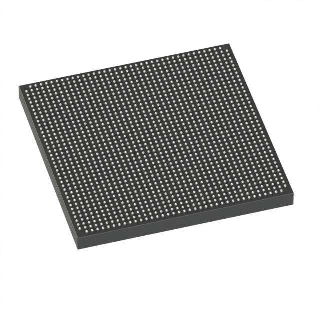
Stratix® V GX Field Programmable Gate Array (FPGA) IC 840 53248000 840000 1932-BBGA, FCBGA |
|---|---|
| Quantity | 72 Available (as of June 15, 2026) |

| Product Category | Field Programmable Gate Array (FPGA) |
|---|---|
| Manufacturer | Intel |
| Manufacturing Status | Obsolete |
| Manufacturer Standard Lead Time | Contact Us |
| Datasheet |
Specifications & Environmental
| Device Package | 1932-FBGA, FC (45x45) | Grade | Industrial | Operating Temperature | -40°C – 100°C | ||
|---|---|---|---|---|---|---|---|
| Package / Case | 1932-BBGA, FCBGA | Number of I/O | 840 | Voltage | 820 mV - 880 mV | ||
| Mounting Method | Surface Mount | RoHS Compliance | RoHS Compliant | REACH Compliance | REACH Unknown | ||
| Moisture Sensitivity Level | 3 (168 Hours) | Number of LABs/CLBs | 317000 | Number of Logic Elements/Cells | 840000 | ||
| Number of Gates | N/A | ECCN | 3A001A2C | HTS Code | 8542.39.0001 | ||
| Qualification | N/A | Total RAM Bits | 53248000 |
Overview of 5SGXMA9N3F45I4N – Stratix V GX FPGA, 840,000 Logic Elements, ~53.248 Mbits RAM
The 5SGXMA9N3F45I4N is a Stratix® V GX field-programmable gate array (FPGA) offered for industrial-grade applications. It provides a high-density logic fabric with substantial on-chip memory and a large I/O count, delivered in a 1932-ball FCBGA package suitable for surface-mount assembly.
Engineered for designs that require large logic capacity, abundant embedded memory, and broad external connectivity, this device targets complex digital systems in industrial and high-performance embedded markets.
Key Features
- Logic Capacity — 840,000 logic elements (LEs) to implement large-scale digital designs and complex hardware architectures.
- Embedded Memory — Approximately 53.248 Mbits of on-chip RAM for buffering, packet processing, and data-path storage.
- I/O Density — 840 user I/Os to support extensive peripheral and high-pin-count interface requirements.
- Power and Operating Range — Core voltage supply range of 820 mV to 880 mV, enabling defined core power delivery profiles for board-level power design.
- Package & Mounting — 1932-BBGA (FCBGA) supplier device package (1932-FBGA, FC 45×45), surface-mount mounting type for compact board integration.
- Temperature & Grade — Industrial grade with an operating temperature range of –40 °C to 100 °C for deployment in demanding environments.
- Standards Compliance — RoHS compliant, meeting common environmental directives for component selection and manufacturing.
- Stratix V GX Family Context — Part of the Stratix V GX series, which the datasheet describes with transceiver and speed-grade options for multi-gigabit channel configurations (refer to the official datasheet for family-level transceiver speed grades and options).
Typical Applications
- Industrial Control & Automation — Implement complex control algorithms, real-time processing, and large I/O interfacing for factory automation and equipment control.
- High-Performance Embedded Systems — Deploy as the central programmable fabric for compute- and data-intensive embedded platforms that require large logic and memory resources.
- Communications Infrastructure — Use the device’s high I/O count and Stratix V GX family transceiver options for protocol processing and board-level aggregation tasks.
- Signal Processing — Leverage dense logic and on-chip RAM for buffering and pipeline implementation in DSP, video, or sensor-processing pipelines.
Unique Advantages
- High logic density: 840,000 logic elements enable integration of extensive custom logic and IP blocks on a single device, reducing board-level complexity.
- Substantial embedded memory: Approximately 53.248 Mbits of on-chip RAM supports large buffers, FIFOs, and state storage without relying solely on external memory.
- Extensive I/O resources: 840 I/Os provide flexibility to interface with multiple peripherals, parallel buses, and high-pin-count connectors.
- Industrial temperature rating: Operation from –40 °C to 100 °C suits deployment in environments with wide thermal variation.
- Board-level form factor: 1932-ball FCBGA package and surface-mount mounting optimize board density and mechanical robustness for complex PCBs.
- Regulatory readiness: RoHS compliance supports environmentally conscious manufacturing and reduces material-restriction concerns.
Why Choose 5SGXMA9N3F45I4N?
The 5SGXMA9N3F45I4N balances very large logic capacity and meaningful embedded memory with a high I/O count and industrial operating range, making it a strong candidate for designs that consolidate multiple functions onto a single FPGA. Its package and surface-mount form factor enable compact, production-ready board layouts.
This device suits engineering teams developing complex embedded, industrial, and communications systems that require scalable logic resources, on-chip memory for high-throughput data paths, and broad external connectivity, while adhering to RoHS requirements.
If you would like pricing, availability, or to submit a purchase inquiry for 5SGXMA9N3F45I4N, please request a quote or submit an RFQ through your preferred procurement channel.


Date Founded: 1968
Headquarters: Santa Clara, California, USA
Employees: 130,000+
Revenue: $54.23 Billion
Certifications and Memberships: ISO9001:2015, ISO14001:2015, ISO17025:2017, ISO27001:2022, ISO45001:2018, ISO50001:2018


