
5SGXMB5R2F43C1N
| Part Description |
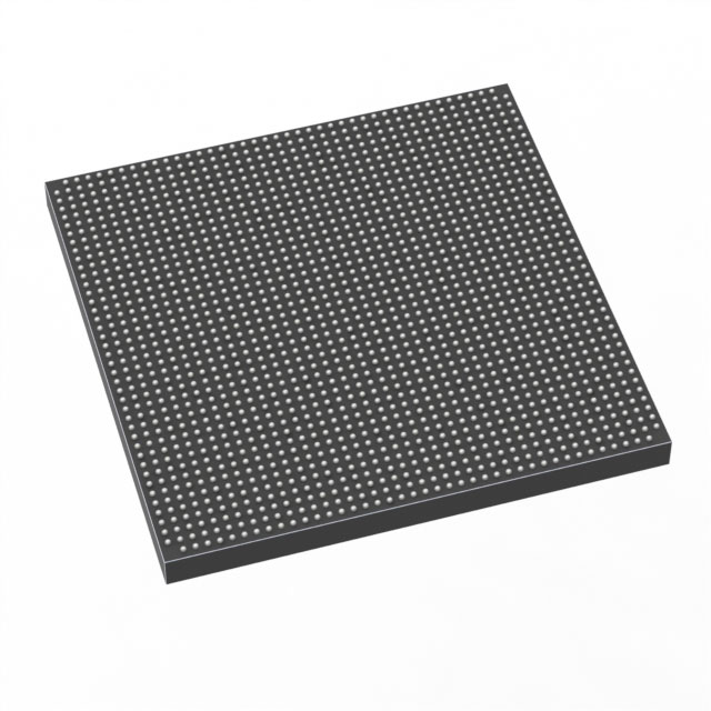
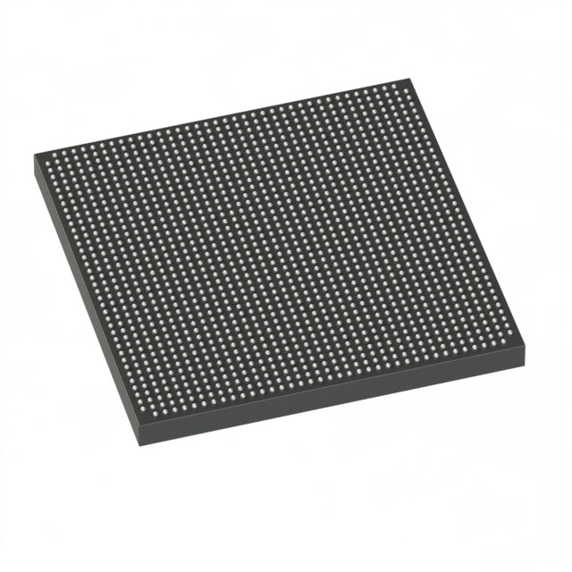
Stratix® V GX Field Programmable Gate Array (FPGA) IC 600 41984000 490000 1760-BBGA, FCBGA |
|---|---|
| Quantity | 29 Available (as of June 15, 2026) |

| Product Category | Field Programmable Gate Array (FPGA) |
|---|---|
| Manufacturer | Intel |
| Manufacturing Status | Obsolete |
| Manufacturer Standard Lead Time | Contact Us |
| Datasheet |
Specifications & Environmental
| Device Package | 1760-FCBGA (42.5x42.5) | Grade | Commercial | Operating Temperature | 0°C – 85°C | ||
|---|---|---|---|---|---|---|---|
| Package / Case | 1760-BBGA, FCBGA | Number of I/O | 600 | Voltage | 870 mV - 930 mV | ||
| Mounting Method | Surface Mount | RoHS Compliance | RoHS Compliant | REACH Compliance | REACH Unknown | ||
| Moisture Sensitivity Level | 3 (168 Hours) | Number of LABs/CLBs | 185000 | Number of Logic Elements/Cells | 490000 | ||
| Number of Gates | N/A | ECCN | 3A001A2C | HTS Code | 8542.39.0001 | ||
| Qualification | N/A | Total RAM Bits | 41984000 |
Overview of 5SGXMB5R2F43C1N – Stratix® V GX Field Programmable Gate Array (FPGA) IC
The Intel 5SGXMB5R2F43C1N is a Stratix V GX Field Programmable Gate Array in a 1760-FCBGA package (42.5 × 42.5 mm), supplied as a commercial-grade device. It delivers large programmable logic capacity and substantial embedded memory in a surface-mount FCBGA package for designs requiring high logic density and extensive I/O.
Designed for applications that need significant on-chip resources, this device combines 490,000 logic elements with approximately 42 Mbits of embedded memory and up to 600 I/O pins, while operating from a core supply of 870 mV to 930 mV and within a commercial temperature range of 0 °C to 85 °C.
Key Features
- Logic Capacity 490,000 logic elements (cells) to support complex programmable logic and large-scale design implementation.
- Embedded Memory Approximately 42 Mbits of on-chip RAM for local storage, buffering, and memory-intensive logic functions.
- I/O Density Up to 600 I/O pins to support extensive peripheral and board-level connectivity.
- Power and Core Supply Core voltage range specified at 870 mV to 930 mV to match system power budgets and core requirements.
- Package 1760-FCBGA (1760-BBGA) package case, 42.5 × 42.5 mm, providing a high-density, surface-mount form factor.
- Temperature Grade Commercial grade operation from 0 °C to 85 °C for standard temperature environments.
- Mounting and Compliance Surface-mount device with RoHS compliance for lead-free manufacturing processes.
- Family Reference (Datasheet) Stratix V GX device-level electrical and transceiver characteristics are documented in the provided device datasheet for detailed implementation guidance.
Typical Applications
- High-density FPGA designs Applications that require extensive programmable logic and embedded memory benefit from the 490,000 logic elements and ~42 Mbits of on-chip RAM.
- High I/O systems Systems requiring broad signal interfacing and complex board-level connections can take advantage of up to 600 I/O pins.
- Platform prototyping and acceleration Large logic capacity and substantial memory make this device suitable for prototyping and hardware acceleration tasks that need significant on-chip resources.
Unique Advantages
- Large programmable capacity: 490,000 logic elements enable implementation of complex designs and large-scale logic integration.
- Substantial embedded memory: Approximately 42 Mbits of on-chip RAM reduces dependence on external memory for many buffering and state-storage functions.
- High I/O count: Up to 600 I/O pins support dense interfacing and integration with multiple peripherals or board subsystems.
- Compact high-density package: 1760-FCBGA (42.5 × 42.5 mm) provides a surface-mount, high-pin-count solution for space-constrained designs.
- Commercial temperature and RoHS compliance: Rated for 0 °C to 85 °C and RoHS-compliant for standard commercial deployments and lead-free manufacturing.
- Defined core power envelope: Core supply range of 870 mV to 930 mV enables predictable power provisioning in system designs.
Why Choose 5SGXMB5R2F43C1N?
The 5SGXMB5R2F43C1N positions itself as a solution for designs that demand high logic density, significant on-chip memory, and large I/O capacity in a commercial-grade FPGA. Its combination of 490,000 logic elements, approximately 42 Mbits of embedded RAM, and up to 600 I/O pins provides a balanced platform for complex programmable designs implemented in a compact 1760-FCBGA surface-mount package.
This device is suited to engineering teams and system designers who need scalable FPGA resources with clearly defined electrical and thermal operating windows. The available device datasheet documents family-level electrical characteristics and transceiver information to support design integration and performance planning.
Request a quote or submit an inquiry to purchase the 5SGXMB5R2F43C1N and receive pricing and availability information for your project requirements.


Date Founded: 1968
Headquarters: Santa Clara, California, USA
Employees: 130,000+
Revenue: $54.23 Billion
Certifications and Memberships: ISO9001:2015, ISO14001:2015, ISO17025:2017, ISO27001:2022, ISO45001:2018, ISO50001:2018


