
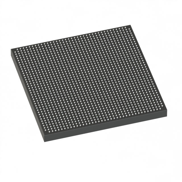
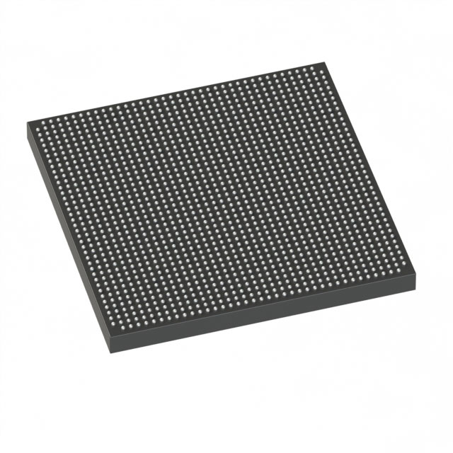
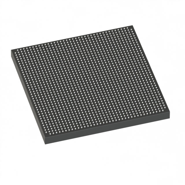
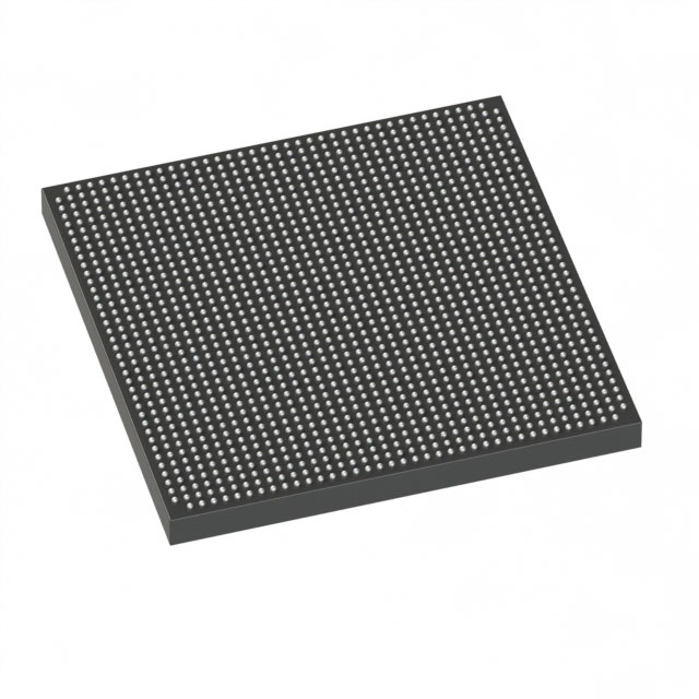
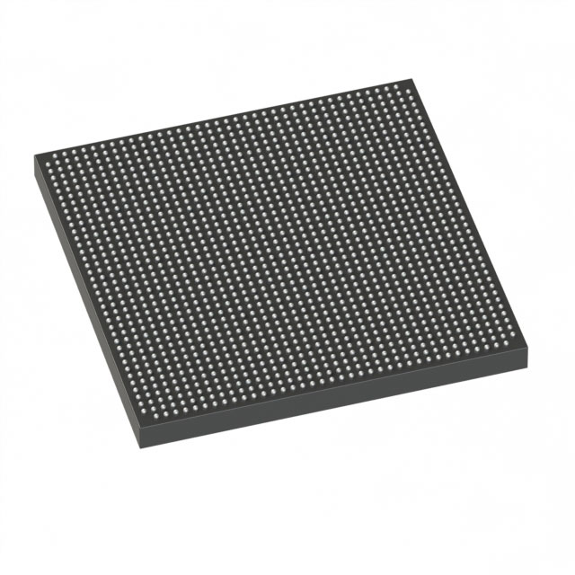
5SGXMB5R3F40C3G
| Part Description |
Stratix® V GX Field Programmable Gate Array (FPGA) IC 432 41984000 490000 1517-FBGA (40x40) |
|---|---|
| Quantity | 1,247 Available (as of October 8, 2026) |
| Product Category | Field Programmable Gate Array (FPGA) |
|---|---|
| Manufacturer | Intel |
| Manufacturing Status | Active |
| Manufacturer Standard Lead Time | 26 Weeks |
| Datasheet |
Specifications & Environmental
| Device Package | 1517-FBGA (40x40) | Grade | Commercial | Operating Temperature | 0°C – 85°C | ||
|---|---|---|---|---|---|---|---|
| Package / Case | 1517-FBGA (40x40) | Number of I/O | 432 | Voltage | 820 mV - 880 mV | ||
| Mounting Method | Surface Mount | RoHS Compliance | RoHS Compliant | REACH Compliance | REACH Unaffected | ||
| Moisture Sensitivity Level | 3 (168 Hours) | Number of LABs/CLBs | 185000 | Number of Logic Elements/Cells | 490000 | ||
| Number of Gates | N/A | ECCN | N/A | HTS Code | N/A | ||
| Qualification | N/A | Total RAM Bits | 41984000 |
Overview of 5SGXMB5R3F40C3G – Stratix® V GX FPGA, 1517-FBGA (40×40)
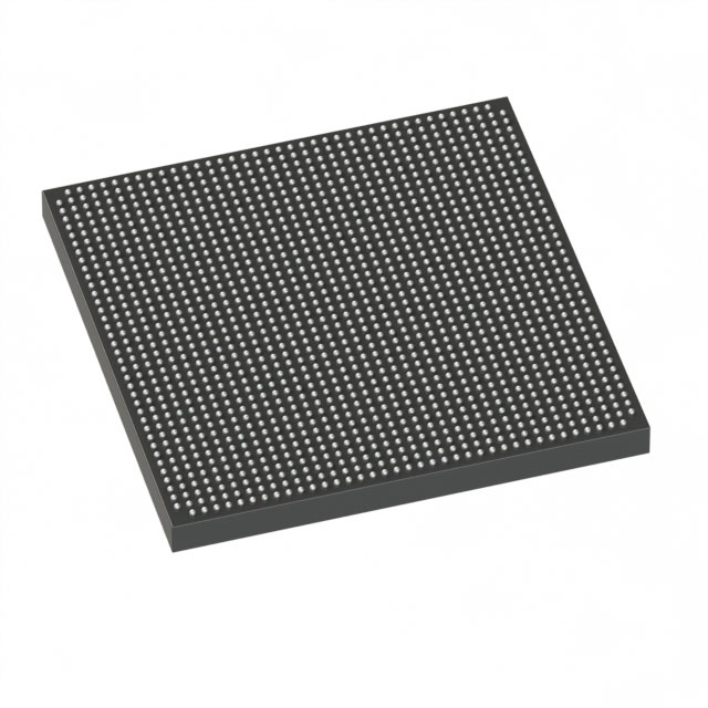
The 5SGXMB5R3F40C3G is an Intel Stratix® V GX field programmable gate array supplied in a 1517‑FBGA (40×40) surface‑mount package. This commercial‑grade FPGA delivers high logic capacity, substantial on‑chip memory, and extensive I/O for demanding digital designs that require programmable hardware resources and flexible system integration.
Key use cases for this device include complex digital signal processing, protocol bridging and packet processing, and high‑density logic implementation where large embedded memory and abundant I/O are required. The device operates from a low core supply range and is RoHS compliant.
Key Features
- Logic Capacity Approximately 490,000 logic elements to implement large, complex designs and multi‑module systems on a single device.
- Embedded Memory Approximately 42 Mbits of on‑chip RAM to support large buffers, FIFOs, and memory‑intensive algorithms without external memory.
- I/O Resources 432 user I/O pins to enable broad peripheral and bus connectivity across the board-level design.
- High‑Speed Transceiver Options (GX) Stratix V GX family devices include transceiver speed grades (family documentation lists channel options including 14.1 Gbps and 12.5 Gbps), enabling high‑speed serial links where required by the application.
- Power and Voltage Core supply range of 0.820 V to 0.880 V, supporting low‑voltage core operation as specified in the device data.
- Package and Mounting 1517‑FBGA (40×40) surface‑mount package for compact board footprint and high pin density.
- Commercial Temperature Grade Rated for 0 °C to 85 °C operation, suitable for commercial electronic products and controlled environments.
- Regulatory Compliance RoHS compliant, meeting common environmental requirements for lead‑free assemblies.
Unique Advantages
- High logic density: The device’s ~490,000 logic elements reduce the need for multiple FPGAs in complex designs, simplifying board layout and system partitioning.
- Large on‑chip memory: Approximately 42 Mbits of embedded RAM supports deep buffering and memory‑centric algorithms without immediate dependence on external DRAM.
- Extensive I/O count: 432 I/Os provide flexibility for parallel interfaces, multi‑channel data acquisition, and mixed I/O standards on a single device.
- Compact, production‑friendly package: 1517‑FBGA (40×40) surface‑mount packaging offers high pin density in a compact footprint for space‑constrained designs.
- Low core voltage: Core supply range of 0.82–0.88 V helps enable efficient core power management consistent with modern FPGA power architectures.
- RoHS compliance: Facilitates integration into lead‑free product lines and supports environmental compliance goals.
Why Choose 5SGXMB5R3F40C3G?
The 5SGXMB5R3F40C3G positions itself as a high‑capacity, commercially rated Stratix V GX FPGA option for engineers who need significant logic resources, abundant embedded memory, and broad I/O in a compact BGA package. Its specification set is suited to designs that demand high integration density and on‑chip memory capacity while operating within standard commercial temperature ranges.
Choosing this device provides scalability within the Stratix V GX family, access to Intel’s device documentation and development flow, and a hardware platform that supports high‑speed serial transceiver options as described in the family datasheet.
Request a quote or submit an inquiry to obtain pricing, lead time, and availability for the 5SGXMB5R3F40C3G.





















Date Founded: 1968
Headquarters: Santa Clara, California, USA
Employees: 130,000+
Revenue: $54.23 Billion
Certifications and Memberships: ISO9001:2015, ISO14001:2015, ISO17025:2017, ISO27001:2022, ISO45001:2018, ISO50001:2018


