
5SGXMB5R3F40C2LN
| Part Description |
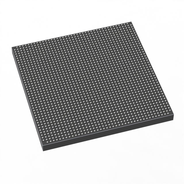
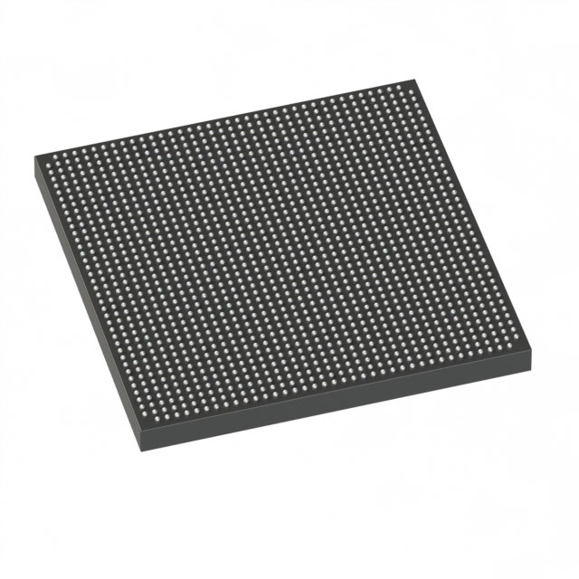
Stratix® V GX Field Programmable Gate Array (FPGA) IC 432 41984000 490000 1517-FBGA (40x40) |
|---|---|
| Quantity | 1,559 Available (as of June 18, 2026) |

| Product Category | Field Programmable Gate Array (FPGA) |
|---|---|
| Manufacturer | Intel |
| Manufacturing Status | Obsolete |
| Manufacturer Standard Lead Time | Contact Us |
| Datasheet |
Specifications & Environmental
| Device Package | 1517-FBGA (40x40) | Grade | Commercial | Operating Temperature | 0°C – 85°C | ||
|---|---|---|---|---|---|---|---|
| Package / Case | 1517-FBGA (40x40) | Number of I/O | 432 | Voltage | 820 mV - 880 mV | ||
| Mounting Method | Surface Mount | RoHS Compliance | RoHS Compliant | REACH Compliance | REACH Unknown | ||
| Moisture Sensitivity Level | 3 (168 Hours) | Number of LABs/CLBs | 185000 | Number of Logic Elements/Cells | 490000 | ||
| Number of Gates | N/A | ECCN | 3A001A2C | HTS Code | 8542.39.0001 | ||
| Qualification | N/A | Total RAM Bits | 41984000 |
Overview of 5SGXMB5R3F40C2LN – Stratix® V GX Field Programmable Gate Array (FPGA) IC 432 41984000 490000 1517-FBGA (40x40)
The 5SGXMB5R3F40C2LN is an Intel Stratix V GX family FPGA providing a large programmable fabric designed for high-density logic and memory integration. It combines 490,000 logic elements with substantial on-chip RAM to support complex, consolidated digital designs.
Targeted at commercial applications, this device is supplied in a compact 1517-FBGA (40×40) surface-mount package and operates across a core supply range of 820 mV to 880 mV and an ambient temperature range of 0°C to 85°C. Detailed electrical and switching characteristics are documented for designers working with the Stratix V device family.
Key Features
- Core Capacity 490,000 logic elements (cells) for implementing large-scale digital functions and complex logic architectures.
- Embedded Memory Approximately 42 Mbits of on-chip RAM (total RAM bits: 41,984,000) to support data buffering, FIFOs, and local storage without external memory.
- I/O Resources 432 I/O pins to enable broad system interfacing and flexible board-level connectivity.
- Power Range Core voltage supply specified from 820 mV to 880 mV, allowing integration within tight power-rail budgets.
- Package & Mounting 1517-FBGA (40×40) surface-mount package suitable for compact, high-density PCB designs.
- Temperature Grade Commercial grade operation from 0°C to 85°C, matching standard commercial electronics environments.
- Compliance RoHS compliant to meet environmental and regulatory requirements for lead-free assembly.
Typical Applications
- High-density digital systems Implement large combinational and sequential logic blocks where a high count of logic elements is required.
- Memory-intensive designs Use the device’s approximately 42 Mbits of embedded RAM for buffering, packet storage, and on-chip data structures.
- I/O-rich interfaces Leverage 432 I/Os for multi-channel peripherals, board-level glue logic, and broad sensor/actuator interfacing.
- Board-level prototyping and integration Compact FBGA package and surface-mount mounting make it suitable for dense PCB layouts and evaluation platforms.
Unique Advantages
- High logic density: 490,000 logic elements reduce the need for multiple devices, simplifying system design and lowering board-level complexity.
- Large on-chip memory: Approximately 42 Mbits of embedded RAM supports data buffering and local processing without immediate reliance on external memory.
- Extensive I/O capability: 432 I/Os provide flexibility for complex interfacing and parallel connectivity across subsystems.
- Compact packaging: The 1517-FBGA (40×40) surface-mount package balances footprint and pin count for dense designs.
- Commercial readiness: Rated for 0°C to 85°C operation and RoHS compliant for standard commercial product deployments.
Why Choose 5SGXMB5R3F40C2LN?
The 5SGXMB5R3F40C2LN positions itself as a high-capacity Stratix V GX FPGA option for commercial designs that require substantial programmable logic, significant embedded RAM, and broad I/O. Its specification set—490,000 logic elements, approximately 42 Mbits of on-chip RAM, 432 I/Os, and a compact 1517-FBGA package—supports consolidation of complex digital functions onto a single device.
Designers seeking a documented Stratix V solution for commercial applications will benefit from the device’s clearly defined electrical characteristics and operating ranges. The part is suited for teams focused on scalable, on-chip integration where logic density, embedded memory, and flexible interfacing are primary design drivers.
Request a quote or submit a procurement inquiry to receive pricing, lead-time, and availability information for the 5SGXMB5R3F40C2LN.


Date Founded: 1968
Headquarters: Santa Clara, California, USA
Employees: 130,000+
Revenue: $54.23 Billion
Certifications and Memberships: ISO9001:2015, ISO14001:2015, ISO17025:2017, ISO27001:2022, ISO45001:2018, ISO50001:2018


